Scaling the DAC output?

matherp

Senior Member
One for the analogue experts:

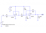
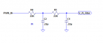
I want to produce a voltage between 2.2 and 3.5 volts with around 5ma drive capability from the DAC on a 08M2. I'm using the internal voltage reference FVR4096 as the +ve input to the DAC

If I just put the DAC output into a rail-to-rail opamp (MCP612). Then I can only use 11 levels (15-25). I need around double this for the application.

So I need to scale the DAC output by a factor of 1.3/4.096 and add a 2.2V bias voltage. I tried 75K:18K resistor divider on the input to the opamp, in theory to limit the voltage to around 3.5V, but even that 93Kohm load killed the DAC output.

Help appreciated

Thanks

Peter
 

g6ejd

Senior Member
Use two op-amps, the first being a non-inverting buffer stage (input to +) and 100% feedback, that will solve the impedance mismatch, but it is another Op-Amp. You can get two in a packaged though.

You could scale up the values to 750K and 180K, but still may not be enough.
 

premelec

Senior Member
I haven't done it but it looks like you can use FVRSETUP to vary the DAC top voltage to vary the range of the output into more steps if you need to - the down side is to have to call FVRSETUP changes which may produce some glitches - perhaps this helps - I've only used external 8 bit DACs set by serial from the PICAXE. [and there's always PWMOUT with a smoothing filter...]
 

AllyCat

Senior Member
Hi,

The output impedance of the DAC varies from about 5k up to 40k ohms over its output range (it's basically a 160k potentiomter) so a buffer amplifier is required in most cases. However, when connected to an op-amp's + input the minimum gain achieveable is unity (higher gains use a potential divider in the feedback path). Therefore, IMHO, it would be better to use the FVR1024 or 2048 reference so that the DAC can be followed by an op-amp configuration with a gain equal to or slightly above 1. Note that FVR1024 is the "accurate" reference, the other two are created by x2 and x4 internal amplification.

But you still need to "sit up" the output voltage using a bias network. Is the supply rail sufficiently accurate to define this? Do you have a specification for your required DAC output voltage? For example how fast must it respond and must the "steps" be equal in amplitude? Sometimes "loading" the DAC output pin can be acceptable, because the "readDAC" command can report the actual output voltage. And of course PWM can give far higher resolution (10 bits versus 5 bits) and not on a pin shared with the Serial/Programming Output.

Cheers, Alan.
 

westaust55

Moderator
Since you are already considering to add external (op-amp) components, consider an external i2c controlled DAC. These are available with 64, 128 and 256 step variants.
What is the load on the analogue output?
Maybe even a digital pot. These allow you to tie the resistor to an alternate supply so you can use more of the step range for greater resolution.

I have posts some info in the past on this forum for both DACs and Dig-Pots.
 

Goeytex

Senior Member
This should get you close using a common dual op amp. I used an LM358 in the Spice Sim, but a good rail to rail will allow a supply of less than 5V.
 

Attachments

matherp

Senior Member
Many thanks for the great suggestions.

I'll start experimenting today and report back progress. The circuit is to provide input to a motor controller on an e-bike. I'm trying to combine both a hand throttle and a hall effect pedal sensor. Why the motor controller has this voltage range I don't know, probably because the supplied rudimentary throttle doesn't use a rail-to-rail op amp and the motor controller needs a fair voltage to turn on at all.

Seems like there are three options:
1: use Goeytex's two stage circuit to first buffer the DAC and then add in the offset. I had missed the idea of using FVR1024 to allow amplification in the adder second stage - thanks for that, and for modelling it!
2: use PWM. I'll start by trying a 100K resistor into a 0.1uF capacitor on the input to opamp and see if that gives me the results I want.
3: buy a i2c DAC. I've got an 8-pin SPI DAC (MCP4822) but that means going to a 14M2 to give me enough pins to drive it. A quick scan of RS looks like i2c DACs start at £5+, i2c digital pots are much cheaper but then also need the buffering opamp, so this will be the last option.

Thanks again

Peter
 
Last edited:

AllyCat

Senior Member
Hi Peter,

Presumably the motor supply rail (battery) voltage will vary with the state of (dis)charge? So the optimum design may depend on how (or if) you need the control voltage to vary with that voltage. The DAC output (referenced to FVR_xxxx) should be stable, but the "bias" component will be proprtional to the (Op-Amp) supply rail. Low-Pass-Filtered PWM of course would "track" the PICaxe supply rail.

If you need to re-allocate pin C.2 to its PWM function, then it's possible to "work around" the PICaxe limitation of C.0 being an "output only" and use it even as an analogue input, if required.

Cheers, Alan.
 

matherp

Senior Member
After testing I have gone with the PWM route. 100K resistor into 0.47uF capacitor as the filter and then into the MCP612 opamp to provide the drive. This produces a very clean signal on the scope, was easy to calibrate in the code, is fast enough for the application, and gives me plenty of resolution (100 levels)
Using the DAC on a 08M2 is a bit painful as it shares the pin with serout which mean plugging and unplugging the serial cable repeatedly and also often having to do hard resets to get it to program. Goeytex's design works well (I used a MCP602 opamp to test) but without installing trimmers rather than fixed resistors would take a bit of fiddling values to calibrate.
The e-bike uses one of the cyclone motors (http://www.cyclone-tw.com/). The built-in motor controller provides a clean 5V supply so the picaxe circuit uses this and inputs the control signal from the existing throttle (voltage) and outputs a replacement composite based on either the throttle or hall effect sensors on the crank. Cyclone provide a pedal sensor, but the version I had just stops the motor if you are not pedalling, whereas my design uses the pedals as a proportional throttle. I use 8 magnets on a crank mounted disk to trigger the hall switch (allegro 3144). If anyone is interested I can provide more details.
Thanks again to all for the help

Peter
Code:
#picaxe 08m2
#no_data
symbol dacmin=155 ' value of pwm duty to give maximum voltage to the controller that doesn't start the motor
symbol dacmax=255 ' value of pwm duty to give full throttle
symbol dacscale=dacmax-dacmin
symbol slowpulse = 55000 ' pulse duration while pedalling slow enough to not start the motor
symbol fastpulse = 20000 'pulse duration above which full throttle is applied
symbol slowscale=slowpulse-fastpulse
symbol slowcalc=slowscale/1000
symbol minadc = 40 ' lowest adc value given by the throttle
symbol maxadc = 220 'highest adc value given by the throttle
symbol adcscale=maxadc-minadc
symbol controlleroff = 30 ' adc value below which the controller is switched off
symbol throttlein=w1
symbol pedalin=w2
symbol s1=b6
symbol s2=b7
symbol s3=b8
'
setfreq m4
adcsetup=1
pwmout C.2, 99, 0
'
do 

	readadc c.1,s1
	readadc c.1,s2
	readadc c.1,s3
	throttlein=s1+s2+s3/3
'	sertxd ("Throttle ",#throttlein,cr,lf)
	if throttlein > controlleroff then 'only execute if controller not switched off
		throttlein=throttlein min minadc 'shouldn't be lower than this but force it anyway
		throttlein = throttlein max maxadc ' shouldn't be higher than this but force it anyway
		throttlein=throttlein - minadc * dacscale / adcscale + dacmin
		pulsin c.3,1,pedalin 'check for next pulse created by a pedal stroke or timeout
		sertxd ("Pedal ",#pedalin,cr,lf)
		if pedalin <>0 then 'not timed out
			pedalin=pedalin min fastpulse - fastpulse /1000 * dacscale /slowcalc 
			pedalin=pedalin max dacscale
			pedalin=dacmax-pedalin
		else 'timed out
			pedalin=dacmin
		endif
		if throttlein>pedalin then
			pwmduty c.2, throttlein
		else
			pwmduty c.2, pedalin
		endif
	else
		pwmduty c.2,0
	endif
'	sertxd (#throttlein," ",#pedalin,cr,lf)
loop
 

Goeytex

Senior Member
Glad you found a good solution.

To make an improvement, you might consider a simple upgrade to the 100K/.47u low pass filter. As a PWM integrator, A pi filter will provide reduced ripple and much better response.
 

Attachments

wapo54001

Senior Member
Glad you found a good solution.

To make an improvement, you might consider a simple upgrade to the 100K/.47u low pass filter. As a PWM integrator, A pi filter will provide reduced ripple and much better response.
Your example uses 40% of the resistance of matherp's 100K, and somewhat less total capacitance than the .47uF of his circuit. And this provides better ripple control and faster response (settling time) to changes in PWM drive?
 

Goeytex

Senior Member
Your example uses 40% of the resistance of matherp's 100K, and somewhat less total capacitance than the .47uF of his circuit. And this provides better ripple control and faster response (settling time) to changes in PWM drive?
Yes it does.
 

wapo54001

Senior Member
This concept is potentially very useful for me. I went to the Okawa Denshi website and didn't get much out of it, because I couldn't relate the two stage filter information to the single stage filter information very well given the information as presented.

I found this website: http://http://www.electronics-tutorials.ws/filter/filter_2.html

which helped me a lot. However, it discussed first and second order filters and a first order integrator but did not discuss a second order integrator.

Also, this website seems to indicate that the second stage resistor and capacitor values should be markedly different from the first stage values:

"In practice, cascading passive filters together to produce larger-order filters is difficult to implement accurately as the dynamic impedance of each filter order affects its neighbouring network. However, to reduce the loading effect we can make the impedance of each following stage 10x the previous stage, so R2 = 10 x R1 and C2 = 1/10th C1."

Is this rule useful in designing a two-stage integrator, or does it not apply? Perhaps this is too far off topic but I'd like to know how 2-stage integrator improve response time over a single stage integrator?
 

fernando_g

Senior Member
"In practice, cascading passive filters together to produce larger-order filters is difficult to implement accurately as the dynamic impedance of each filter order affects its neighbouring network. However, to reduce the loading effect we can make the impedance of each following stage 10x the previous stage, so R2 = 10 x R1 and C2 = 1/10th C1."

Is this rule useful in designing a two-stage integrator, or does it not apply? Perhaps this is too far off topic but I'd like to know how 2-stage integrator improve response time over a single stage integrator?
This rule minimizes, although it does not completely eliminate, the interaction between the two stages. For your application, which doesn't require a very accurate fc, it is perfectly fine.
Now, and this is important: the load you apply to the output will also have an effect. Again, you may live with that limitation if the output load is at least 10X (R1 + R2).

Me? I would use a single stage, 2nd order active filter, but that is only me.
 

wapo54001

Senior Member
@fernando_g, thank you for the clarification.

For me, the load is a mosfet gate but board space is an issue so will consider the simpler 2nd order filter without the active element. I'm assuming that if my goal is to get as close to ripple-free DC as is reasonably possible then using two same-value stages with an equally large capacitor in the second stage is the way to minimize the ripple at the output.

In my current arrangement I am using 1 mega ohm into 2.2 uF tantalum (not enough room for film) because that combination has the correct rate-of-change for my application. If I could use different values and achieve the same rate-of-change but end up with smaller ripple at the output, that would be worth implementing.
 
Top