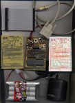
This project provides a socket for a PICAXE-40 that can be programmed with Revelation’s BASIC Editor/Compiler/Programmer/Simulator/System-Monitor/Debugger. This Project also has provisions for several passives and has sockets for other useful IC. See photo.
This Project is small, light and cheap and is tailored for a PICAXE-40X1. It is about the size of a credit card, it weights about an ounce and this project has an initial cost of under $40US which includes the PWB ($20), the 7805, PICAXE-40X1, Ceramic Resonator and all the rest of the discretes. Actual Size: 3.8” X 2.5”.
The schematic is nothing special, it is the chaining together of several Vendor Application Notes, the PWB Artwork is unique and I put it in the Public Domain for anyone that wants to copy it.
This project also provides sockets for eight I2C Memory chips, plus one other I2C socket that can be used for a Real Time Clock and a socket for a +/- 10V Charge Pump that can be an up to a 100 ma power supply for other things. The I2C and One-Wire lines are taken to the I/O Board.
Parts List for PICAXE Processor Board Version G:
C1 10UU@50VWDC Jameco 852473 or Radio Shack # 27-1025
C2 .001U@50WVDC Jameco 15192 or Radio Shack # 27-210126
C3 0.01U@35WVDC Jameco 15231 or Radio Shack # 27-21065
C4 22U@35WVDC Jameco 545887 or Radio Shack # 27-21026
*C5 0.1U@35WVDC Jameco 545561 or Radio Shack # 27-21069
*C6 22U@35WVDC or any value above 1U Jameco 545561 or Radio Shack # 27-21026
*C7 22U@35WVDC or any value above 1U Jameco 545561 or Radio Shack # 27-21026
C8 0.01U@35WVDC Jameco 15231 or Radio Shack # 27-21065
C9 0.01U@35WVDC Jameco 15231 or Radio Shack # 27-21065
C10 0.01U@35WVDC Jameco 15231 or Radio Shack # 27-21065
*C11 22U@35WVDC or any value above 1U Jameco 545561 or Radio Shack # 27-21026
*C12 22U@35WVDC or any value above 1U Jameco 545561 or Radio Shack # 27-21026
*C13 1F@5VDC Jameco 227811 used only by the DS1307.
D1 RED LED Radio Shack #27-60041
D2 IN5819 (DO-41 case) Schottky, 40V 1A Digikey #1N5819-E3/STGI-ND
D3 1N4007 (DO-41 case) any power rectifier diode will do, as long as it fits and PIV is OK.
*D4 1N4148 Jameco 36038
DIP-8 Jameco 112206 order enough for locations U2 thru U13.
DIP-8 Oscillator Socket Jameco 676385 can be used in location U13.
DIP-40 Jameco 112311 for location U14.
JP1 3.5mm Stereo female connector Mouser # 806-STX-3500-3C, check foot print.
PWB1 order from EXPRESSPCB
R1 10 K 1/8W 5% Radio Shack 27-11126
R2 22 K 1/8W 5% Radio Shack 27-11128
R3 4.7 K 1/8W 5% Radio Shack 27-11113
R4 330 1/8W 5% Radio Shack 27-11215
R5 180 1/8W 5% Radio Shack 27-11205
*R6 47 K 1/8W 5% Radio Shack 27-11130
*R7 47 K 1/8W 5% Radio Shack 27-11130
*R9 330 1/8W 5% Radio Shack 27-11215
RN1 10 KX10 SIP Jameco 280947
RN2 10 KX10 SIP Jameco 280947
SW1 Push Button Switch NO, Jameco 122973, check foot print.
U1 LM7805 Jameco 786138 or Radio Shack 276-1770
*U3 MAX680 charge pump, +5 to +/-10V Converter
*U4 any I2C memory chip, sockets are hardwired for address extension
sockets are hardwired for either 24FC256, or 24FC512 or 24FC1024.
*U12 any I2C Real Time Clock, socket wired for DS1307
*U13 TTL Crystal Clock Oscillator 30ppm stability, Mouser 520-TCH400-C
U14 PICAXE-40X1 (Enhanced) sales@hvwtech.com or www.microchip.com
X1 4MHz ceramic resonator, Jameco 324697CJ or www.microchip.com
*X2 32.768 Crystal to go with DS1307, Jameco 14584
JP2 RC battery Connector Repair Kit Radio Shack #23-00444, solder the male half to PWB and use female half of this kit for the Wall-Wart power supply.
Programming Cable Any NULL-MODEM cable cut in half and each half along with male 3.5mm Stereo connector makes a programming cable, see schematic for connections.
*I/O Cable Any 50 conductor ribbon cable. Moser 3365/50 .
* indicates item not used on initial project, but PWB is ready to take these components
How to build this PICAXE Project: Download the free software from www.expresspcb.com ; you will need this software to view my schematic and my artwork files as I designed them using this software. Print out the parts list and buy three copies of each part, wait for the parts to come in before ordering the printed wiring board, as you need to double check the part’s foot print against the PWB. When all is OK, order the PWB. Any questions then e-mail me at: bigjoe@valp.net .
Stuff the PWB and solder. For this project U1 is soldered-in, and the PICAXE-40X1 is inserted into U14 socket, the rest of the IC Sockets are reserved for future projects.
How I soldered: Let me tell you how I had to solder this project to make it work, it might save you a wasted board. Everything on this PWB is small and jammed together; the fabrication of this Board is at the high end of the expected Hobbyist Soldering Skill level. Soldering all of these 8-pin DIP sockets is very tiring and frustrating, just one solder blob or bridge will ruin everything, and there are no provisions for re-work. Due to the close spacing on some of the DIP sockets there is a requirement for order of assembly. Here is what I found I had to do to get things to work: insert the sockets for U4, U5 then solder; U6, U7 and U8 then solder; U9 and U10 then solder; U11 and U12 then solder. The rest are easier. I found that I needed to use a bright light and 6X magnifier to see to solder; also a pencil iron with a narrow conical tip, a 0.020 (or 1/32) tip and some 0.031 thin multi-core rosin solder to do this job.
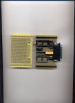
My design philosophy: Put all hardware parts that are not going to change from project to project on the Processor Board. Put anything else on the Interface Board. This PICAXE Project is the Processor Board; from project to project nothing will change further on this PWB, except seating some IC into their sockets and the loading of new software.
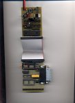
Power All the power is conditioned on the Processor Board and pass from this board to the other boards via the 50 pin ribbon cable.
Programming I put all the components for the programming circuit on this processor board. So to build your own Programming Cable: 1) buy any Null-Modem Cable and 2) cut it in half. 3) On the cut end, bear the wire that is connected to pin 5 on the female DB-9 connector and solder this to the shell of the 3.5mm male stereo connector. 4) Same with DB-9 pin 2 to 3.5mm pin 2 and DB-9 pin 3 to 3.5mm pin 1. Also see the schematic for wiring diagram.
Ups and Downs I use RN1 to pull-down all the PICAXE-40’s ADC pins, this helps reduce noise and I use RN2 to pull-up the Input Pins. If this is not the way you do things, then leave RN1 or RN2 off the board. I use the ADC for analog sensors and I put Op-Amps on the I/O Board for signal conditioning. I use the PICAXE’s Input pins for Digital or Microswitch inputs; the input logical signal will be HIGH with no switch action and with a switch closure, the pin connected to the switch will go LOW for a brief instant. See the PICAXE Users Manual, Section 3, for designing sensor circuits, more in the next project.
Clock Decision: Often, Advanced Micros will give away a free Ceramic Resonator with the purchase of the PICAXE-40. The Ceramic Resonator is great at keeping cost down. But when I am doing Digital Signal Processing or Digital Signal Synthesis, the stability of a Ceramic Resonator is not good enough, so U13 is provided for a crystal oscillator. For DSP, 10ppm or better is desirable; 30ppm is useable; anything above 100ppm will cause problems.
Future: There are a lot of 8-pin DIP sockets on this PWB reserved for future projects. For example U4 thru U11 could be populated with 24FC256 I2C Memory chips for over a Gig of external memory, the I2C address extensions are already hard wired to these sockets. U12 is wired for any I2C chip like a DS1307 Real Time Clock that could be used to time stamp data and all that Memory could be used as a data logger. For a Data Logger, the signal conditioning and cable connectors would be on a separate board which connects to this Processor Board with a 50-pin Ribbon Cable. All the PICAXE-40 I/O pins are brought to the I/O Board so there are lots of I/O pins for the sensor channels. Think Robotics, PID Closed-loop Servos, Factory Automation, MIDI Music, for future projects. With so many I/O pins on the PICAXE-40 the possibilities are very many.
See attachments for schematic and artwork for PWB. You have to rename them to make them work:
ProcessorG1.dsn -> ProcessorG1.sch
ProcessorG2.dsn -> ProcessorG2.pcb
Then open these files with espresspcb.exe
This post has been modified, the schematic, artwork and photos have been moved to another post.
This Project is small, light and cheap and is tailored for a PICAXE-40X1. It is about the size of a credit card, it weights about an ounce and this project has an initial cost of under $40US which includes the PWB ($20), the 7805, PICAXE-40X1, Ceramic Resonator and all the rest of the discretes. Actual Size: 3.8” X 2.5”.
The schematic is nothing special, it is the chaining together of several Vendor Application Notes, the PWB Artwork is unique and I put it in the Public Domain for anyone that wants to copy it.
This project also provides sockets for eight I2C Memory chips, plus one other I2C socket that can be used for a Real Time Clock and a socket for a +/- 10V Charge Pump that can be an up to a 100 ma power supply for other things. The I2C and One-Wire lines are taken to the I/O Board.
Parts List for PICAXE Processor Board Version G:
C1 10UU@50VWDC Jameco 852473 or Radio Shack # 27-1025
C2 .001U@50WVDC Jameco 15192 or Radio Shack # 27-210126
C3 0.01U@35WVDC Jameco 15231 or Radio Shack # 27-21065
C4 22U@35WVDC Jameco 545887 or Radio Shack # 27-21026
*C5 0.1U@35WVDC Jameco 545561 or Radio Shack # 27-21069
*C6 22U@35WVDC or any value above 1U Jameco 545561 or Radio Shack # 27-21026
*C7 22U@35WVDC or any value above 1U Jameco 545561 or Radio Shack # 27-21026
C8 0.01U@35WVDC Jameco 15231 or Radio Shack # 27-21065
C9 0.01U@35WVDC Jameco 15231 or Radio Shack # 27-21065
C10 0.01U@35WVDC Jameco 15231 or Radio Shack # 27-21065
*C11 22U@35WVDC or any value above 1U Jameco 545561 or Radio Shack # 27-21026
*C12 22U@35WVDC or any value above 1U Jameco 545561 or Radio Shack # 27-21026
*C13 1F@5VDC Jameco 227811 used only by the DS1307.
D1 RED LED Radio Shack #27-60041
D2 IN5819 (DO-41 case) Schottky, 40V 1A Digikey #1N5819-E3/STGI-ND
D3 1N4007 (DO-41 case) any power rectifier diode will do, as long as it fits and PIV is OK.
*D4 1N4148 Jameco 36038
DIP-8 Jameco 112206 order enough for locations U2 thru U13.
DIP-8 Oscillator Socket Jameco 676385 can be used in location U13.
DIP-40 Jameco 112311 for location U14.
JP1 3.5mm Stereo female connector Mouser # 806-STX-3500-3C, check foot print.
PWB1 order from EXPRESSPCB
R1 10 K 1/8W 5% Radio Shack 27-11126
R2 22 K 1/8W 5% Radio Shack 27-11128
R3 4.7 K 1/8W 5% Radio Shack 27-11113
R4 330 1/8W 5% Radio Shack 27-11215
R5 180 1/8W 5% Radio Shack 27-11205
*R6 47 K 1/8W 5% Radio Shack 27-11130
*R7 47 K 1/8W 5% Radio Shack 27-11130
*R9 330 1/8W 5% Radio Shack 27-11215
RN1 10 KX10 SIP Jameco 280947
RN2 10 KX10 SIP Jameco 280947
SW1 Push Button Switch NO, Jameco 122973, check foot print.
U1 LM7805 Jameco 786138 or Radio Shack 276-1770
*U3 MAX680 charge pump, +5 to +/-10V Converter
*U4 any I2C memory chip, sockets are hardwired for address extension
sockets are hardwired for either 24FC256, or 24FC512 or 24FC1024.
*U12 any I2C Real Time Clock, socket wired for DS1307
*U13 TTL Crystal Clock Oscillator 30ppm stability, Mouser 520-TCH400-C
U14 PICAXE-40X1 (Enhanced) sales@hvwtech.com or www.microchip.com
X1 4MHz ceramic resonator, Jameco 324697CJ or www.microchip.com
*X2 32.768 Crystal to go with DS1307, Jameco 14584
JP2 RC battery Connector Repair Kit Radio Shack #23-00444, solder the male half to PWB and use female half of this kit for the Wall-Wart power supply.
Programming Cable Any NULL-MODEM cable cut in half and each half along with male 3.5mm Stereo connector makes a programming cable, see schematic for connections.
*I/O Cable Any 50 conductor ribbon cable. Moser 3365/50 .
* indicates item not used on initial project, but PWB is ready to take these components
How to build this PICAXE Project: Download the free software from www.expresspcb.com ; you will need this software to view my schematic and my artwork files as I designed them using this software. Print out the parts list and buy three copies of each part, wait for the parts to come in before ordering the printed wiring board, as you need to double check the part’s foot print against the PWB. When all is OK, order the PWB. Any questions then e-mail me at: bigjoe@valp.net .
Stuff the PWB and solder. For this project U1 is soldered-in, and the PICAXE-40X1 is inserted into U14 socket, the rest of the IC Sockets are reserved for future projects.
How I soldered: Let me tell you how I had to solder this project to make it work, it might save you a wasted board. Everything on this PWB is small and jammed together; the fabrication of this Board is at the high end of the expected Hobbyist Soldering Skill level. Soldering all of these 8-pin DIP sockets is very tiring and frustrating, just one solder blob or bridge will ruin everything, and there are no provisions for re-work. Due to the close spacing on some of the DIP sockets there is a requirement for order of assembly. Here is what I found I had to do to get things to work: insert the sockets for U4, U5 then solder; U6, U7 and U8 then solder; U9 and U10 then solder; U11 and U12 then solder. The rest are easier. I found that I needed to use a bright light and 6X magnifier to see to solder; also a pencil iron with a narrow conical tip, a 0.020 (or 1/32) tip and some 0.031 thin multi-core rosin solder to do this job.
My design philosophy: Put all hardware parts that are not going to change from project to project on the Processor Board. Put anything else on the Interface Board. This PICAXE Project is the Processor Board; from project to project nothing will change further on this PWB, except seating some IC into their sockets and the loading of new software.
Power All the power is conditioned on the Processor Board and pass from this board to the other boards via the 50 pin ribbon cable.
Programming I put all the components for the programming circuit on this processor board. So to build your own Programming Cable: 1) buy any Null-Modem Cable and 2) cut it in half. 3) On the cut end, bear the wire that is connected to pin 5 on the female DB-9 connector and solder this to the shell of the 3.5mm male stereo connector. 4) Same with DB-9 pin 2 to 3.5mm pin 2 and DB-9 pin 3 to 3.5mm pin 1. Also see the schematic for wiring diagram.
Ups and Downs I use RN1 to pull-down all the PICAXE-40’s ADC pins, this helps reduce noise and I use RN2 to pull-up the Input Pins. If this is not the way you do things, then leave RN1 or RN2 off the board. I use the ADC for analog sensors and I put Op-Amps on the I/O Board for signal conditioning. I use the PICAXE’s Input pins for Digital or Microswitch inputs; the input logical signal will be HIGH with no switch action and with a switch closure, the pin connected to the switch will go LOW for a brief instant. See the PICAXE Users Manual, Section 3, for designing sensor circuits, more in the next project.
Clock Decision: Often, Advanced Micros will give away a free Ceramic Resonator with the purchase of the PICAXE-40. The Ceramic Resonator is great at keeping cost down. But when I am doing Digital Signal Processing or Digital Signal Synthesis, the stability of a Ceramic Resonator is not good enough, so U13 is provided for a crystal oscillator. For DSP, 10ppm or better is desirable; 30ppm is useable; anything above 100ppm will cause problems.
Future: There are a lot of 8-pin DIP sockets on this PWB reserved for future projects. For example U4 thru U11 could be populated with 24FC256 I2C Memory chips for over a Gig of external memory, the I2C address extensions are already hard wired to these sockets. U12 is wired for any I2C chip like a DS1307 Real Time Clock that could be used to time stamp data and all that Memory could be used as a data logger. For a Data Logger, the signal conditioning and cable connectors would be on a separate board which connects to this Processor Board with a 50-pin Ribbon Cable. All the PICAXE-40 I/O pins are brought to the I/O Board so there are lots of I/O pins for the sensor channels. Think Robotics, PID Closed-loop Servos, Factory Automation, MIDI Music, for future projects. With so many I/O pins on the PICAXE-40 the possibilities are very many.
See attachments for schematic and artwork for PWB. You have to rename them to make them work:
ProcessorG1.dsn -> ProcessorG1.sch
ProcessorG2.dsn -> ProcessorG2.pcb
Then open these files with espresspcb.exe
This post has been modified, the schematic, artwork and photos have been moved to another post.
Last edited: