PICAXE and PCBs

Dicky Mint

Senior Member
Sorry didn't think!

the three vertical traces which don't go anywhere!

the PICAXE bit is not yet 'plumbed in' yet either
 

MartinM57

Moderator
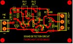
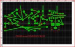
I'm wanting to adopt the star method of PCB design
Why? Just to make life hard for yourself? :)

I might consider star arrangements for ground traces if I was ever worried about ultimate EMI protection - surely not a problem with this circuit - but I certainly wouldn't consider it for every place where traces have to join.

And my PCB OCD can't deal with components and traces not at right angles :( ... and the traces joining at narrow angles are definitely bad news if you were to test your design against standard rules for trace layouts to minimise etching/reliability problems.

I would just join all those three traces together with a horizontal trace - or squeeze the right hand two down between the capacitor pins.

Also, it sounds like you are doing this by hand, and piecemeal if the PICAXE traces are not done yet. That could end in tears and frustration.

IMHO, rather that pursuing star PCB design I would suggest learning a package like Diptrace and use it to draw a schematic, turn that schematic into a board and then try the auto-routing capabilities plus a tidy up by hand afterwards - you can then use the facilities in Diptrace to check that the board design exactly matches the schematic and no traces have been "lost" (I expect you are doing that manually at the moment - and it's hard and error-prone?)
 

Dicky Mint

Senior Member
I was under the, mistaken, belief that one had to join all the equipotential points with uninterupted straight lines to be the star method!

I think I'm perhaps trying to make it too hard for myself

Having not studied PCB design and fabrication at college I have have no real book learning only my experience.

Perhaps I need to take a short course in PCB design?

Rick
 

hippy

Ex-Staff (retired)
I was under the, mistaken, belief that one had to join all the equipotential points with uninterupted straight lines to be the star method!
I believe that's the theory but it soon turns out to be completely impractical for any circuit above minimal complexity.

I am not a PCB design expert but I don't believe star wiring is absolutely necessary except for some specific cases or to overcome particular problems.
 

techElder

Well-known member
I totally agree with Martin. Get DIPTRACE and learn it on the simple boards. Use their auto-routing functions to try different routing methods. Then adjust the routing manually with your experience. Surely a simple circuit can be auto-routed.
 

Dicky Mint

Senior Member
I've never used an auto-router

I spose its high time especialy if I want to design anything more complicated!

I do love my Sprint Layout though!

I intend to keep using it for simple boards as I think it allows for a neat board!

I think I'll temper my idea of star tracing!

Rick
 

ZOR

Senior Member
Why can you not put pads on the ends of the nowhere nodes and have wire links on top of pcb or have I missed something?


?
 

MartinM57

Moderator
...because that's not "star layout"

A true star layout potentially has two pads that are 0.1" apart on one side of the board, travelling independently to the star point with some other connections, which might be 3" away on the other side of the PCB - which is, to be honest, pretty crazy
 

Dicky Mint

Senior Member
@cachomachine

Yup that is the way I have done it up till now, or at least very similar

I have had problems with the PICAXE picking up noise from a motor which is the main reason why I'm investigating "star" routing!

I'll try out my sudo 'star' PCB and see if I get less noise on the ADC pin?

Rick
 
Top