[OT] PCB Design critique

GDSever

Member
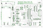
This is somewhat related in that my printed circuit board design is for a Picaxe 28x1 circuit, however I honestly have not designed many circuit boards and am looking for constructive criticism. I've read some sources that indicate PCB traces should look one way, and others that contradict that advice...

So I was hoping to draw on your experience, if possible.

It is a circuit that turns two pumps on and off based on some level switches. One vessel has a high / low switch combination, and the other is used for top-up applications. My intention was to collect information and wirelessly transmit it back to a PC or another Picaxe circuit as well... for now I'm using a 315Mhz transmitter pair from Sparkfun, but hope to ultimately upgrade to the XBee protocol.

Any words of wisdom would be greatly appreciated...
 

Attachments

Dippy

Moderator
I can't comment on the circuit and I have only had the briefest of looks as integrity checking and spacing checking and general layout is your job.

1. I would suggest that your power tracks (+5 and Gnd etc.) are made much fatter where you have long runs.

2. Certainly I would make the tracks to-and-from your fuse holder much wider. You want to ensure that the fuse will pop well before a track does!

3. Sometimes it is good to fill up spaces with Ground (here we go) copper-fill. Though the amount can vary sometimes so I wouldn't like to make the suggestion too general.

4. Is this a photo-resist board you are etching at home? How experienced are you with UV exposure? Or is it guess'n'peel iron on stuff? How good is your printer? How good is your etcher? The PCB: Is it cheap photo-resist board off Ebay or something half decent?

[I merely ask these things because the lower the quality of your product (and/or method) then the higher the chance is that very thin tracks can get etched away. For a home-brew prototype I'd be tempted to fatten up ALL the tracks where possible.]

5. I would also set your pad drill sizes smaller than you intend to actually drill - just for the etching. Just in case of over-exposure or over-etching. And maybe increase the pad sizes marginally. Some cheap board has very poor copper to backing adhesion and pads can fall off if too small.

6. I would be tempted to use rounded-finger style pads on your IC socket so there is a bit more copper 'meat'.

7. I would have much bigger pads on your fuse holder and on that Power Supply thing on the left.

8. Assuming you are using single-sided board this looks like an Autorouted job where you have replaced layer 2 tracks with links. Maybe not, but anyway make those via pads at least 1.8 to 1.9mm diam.

You'll probably get plenty of comments from others who have plenty of spare time, but I'm sure you'll be fine.
 

Mycroft2152

Senior Member
Thats a good looking layout.

Dippy's analysis was excellent. (he must not have hit the Fosters yet)

If you are making the pcb at home then all pads show be oversized. It makes it much easier to drill and prevents the pads from "lifting" during soldering.

The traces should be wider, at least the power rails. Again, if making the board at home, wider traces are more forgiving.

Leaving extra copper on the board is ok, that is just less to remove.

You can always add component legends on the top using toner transfer.

One note: your ULN2803A footprint looks like it is missing a few pins. You realy donl;t want to have tosnip them off or bend them up.

Myc
 
Last edited:

Shack

Member
The overall layout is excellent. It looks like this has an AC PS so the fuse and the trace size is fine. Just double check to be sure the pad matches the hole you intend to drill … bigger hole = bigger pad.

I would re-route the board and set the router to use a 0.020” mil trace min throughout the design and then I would go in manually and increase the ground and 5V rails to 0.025” unless you can route power/ground separately ... looks as though there is plenty of room.

I would also add a 1N4001 diode in the 5v line at the external input to protect the board in the event you use external power.

If you are going to use wire jumpers on the top I would increase the pads for that to a minimum of 0.066” as you will need a decent hole for the wiring.

A larger IC pad would be desirable for a hand drilled hole as Dippy suggests.

Obviously if you intend to control relays you will need a diode across the coil which can be put on the PCB.

You also need by-pass caps on your other IC’s and you may need one on the RF module. The by-pass cap for the 28x1 should be a .1uF and the symbol/pad you have is not correct.
 

hippy

Ex-Staff (retired)
Shouldn't there be some more holes for U4 ?

I'd also suggest more bypass caps, one near the PSU output wouldn't go amiss.

Is this for your own use or are you thinking of providing others with the PCB ? If it's 110V/240V AC in to the fuse etc it's probably worth a "Danger Mains!" legend as well as marking which of the input pins are Live, Neutral and Earth.
 

GDSever

Member
I will fatten traces up, as suggested. I did make the ground and +5V traces thicker than the default setting, but I can bump them up some more... The thing that concerns me a little is the run under the 28x1 since those traces are already somewhat close.

The missing pads on the Darlington driver IC is intentional. I am not planning on snipping the IC itself, but I was planning on using an DIP18 IC socket and snipping its pins... I am only using 2 of the channels on the IC, so the rest are kind of extraneous. Yeah, I could use single darlington pair transistors or something, but I liked the IC approach a little more. Also, the thought of having to drill 12 extra holes, etc seemed crazy, particularly when I could use that "real estate" to run the traces a little wider apart.

I was planning on doing the copper fill... I just hadn't added it into the Diptrace design yet as it is typically a last step.

I am using the photoresist method of exposure using a 2 tube fluorescent light fitted with day bulbs. I have done a couple test runs and have zeroed in on the proper exposure time and methods to get good quality traces. I am using persulphate to etch... The boards are high quality. I have not gone "on the cheap" for any of this particular project, trust me.

No relays are being used - 2 Crydom 5V control 10A SSRs seperate the Picaxe circuit from the 120V for the pumps. Darlington driver channels on U4 control the SSRs.

Excellent comments on the drill hole sizes. Hadn't considered that. I'll be using a Dremel w/ PCB drill bits and the Minicraft tools PZ541 to make the holes...

Thanks for all the input. I know I have missed some of the specific points you all outlined, but trust me that I am digesting and considering all your suggestions. Short on time at the moment, but I'll try to stop back in later and add more. In the meantime, if you're interested in what I'm doing, my blog is http://brewznet.wordpress.com ... All kinds of circuit & homebrewing stuff on there.
 

Dippy

Moderator
"28x1 since those traces are already somewhat close"

- close? That spacing is almost interplanetary Mate :)

If you'd said the spacing was less than 5thou for a Home-Brew then I would have said they're a bit close.
You should be able to get track-track spacing of 10 thou quite nicely. Though I don't know the CAD you use and it's resolution and it's output resolution. I don't know your printer's res either..... maybe 10 thou is too close for your setup. I'd be surprised.

I assume the actual artwork is higher res than your posted image where pads/holes look very 'steppy'?
 

Mycroft2152

Senior Member
DIPTRACE... I thought I recognzed the style. :)

The steppiness is due to the dpi resolution when outputting the drawing as a jpg file for emailing.

When printing from within the program the resolution is based on your printer settings.

One note: when emailing pcb layouts, for other peop[le to use, it is best to print them as pdf's. Other formats will stretch and or shrink the layout and cause problems.

Attached are some examples of the footprints/patterns that work for me.

Myc
 

Attachments

Last edited:

GDSever

Member
Good tips - thanks a ton. Yeah, the low resolution is purely a function of taking a screenshot instead of "printing" to a PDF. The printing resolution looks really great from my inkjet, and while my first attempt was not great (thin traces due to poor board preparation), the second trial run was near perfect. I definitely like the wide pad idea. Very good upgrade...

Getting back to some of the other questions - will be for my own use. I don't think anyone else I know is nuts enough to spend this kind of time, effort and money to automate their brewing grant. I've got the design inside the control box pretty well nailed down and I won't ever open it without killing the power and unplugging first... In fact, since I'll be moving liquids (~150 deg malt sugar water, basically) that control box will only ever be plugged into a GFCI when in use.

The external power screw terminal is actually to test the board out before I solder my $16 power supply and $3 fuse holder down to the board. I'll test it out with some batteries first, make sure it works as expected, then put the big guns in there and remove the battery clip. I suppose if I ever wanted to power something I could use that terminal....

I was planning on using more bypass capacitors, in fact that was the orignal reason for including some extra pads (which ultimately became the +5 and GND rails). I'll be using those, for sure... even though they don't show as a capacitor footprint on the board. I will also take the advice for other capacitors under advisement and update the one for the Picaxe so it shows the correct value... or is it the symbol that is wrong? I assumed a simple ceramic capacitor was all that was needed.

This particular layout and trace was done primarily by hand. I originally used the autorouter for some pieces, but found that Diptrace was not taking advantage of certain things, subtle component shifts made huge simplifications to the traces, and I spent more time correcting the autorouting then just doing it by hand. It also wanted to run traces under the VAA505 power supply, which the owners manual clearly states is a bad idea. Perhaps they meant on the top side of the board... but I figured best to be safe. I went through 8 or 9 iterations of by hand and autorouting... This last one was probably 85% manual. The autorouter feature is really great, but like any tool you have to use it judiciously.

Thanks all for the advice. I really do appreciate it. When I get everything put together (still waiting on the PZ541 drill press stand to arrive - Its killing me having to wait), I'll have to take some pics / video and post something in the projects section.

Prost!
 
Last edited:

wapo54001

Senior Member
I made a very slight change to my last board layout and rendered it "noisy" because I combined the ground (sink) for a warning light -- 100ma -- with the ground for the rest of the picaxe and sensor circuit. Result was that whenever the warning light flashed, the digital readout showing the output of the picaxe integrator circuit became unstable even though I had 100uF on the output of the regulator and .22uF at the Picaxe.)

I built a slightly different card with totally separate grounds for the two circuits that only came together at the ground entrance to the card, and the problem was solved. I came away with the notion that ground traces for power devices should be kept entirely separate from the ground traces for sensitive analog processing circuits. Maybe I just didn't have enough capacitance.
 
Top