One more "proto" PCB

manie

Senior Member
Like Dippy once said, "we all have our quirks". Mine is to "proto" on finished PCB's, you have to trust your design at some time don't you ? I find that this way I blow/sublimate less components than with loose wires on a breadboard.

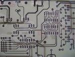
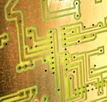
This is my 6th board ever, hopefully the younger members will believe that reasonably good boards can be home brewed, just try it, you'll probably surprise yourself !

Attached is a pic of part of the board.
Manie
 

Attachments

kevrus

New Member
Very nice board. Although prototyping that way is probably not the best, I too have done it (and continue to do so occasionally if truth be told). If it works for you then why not...
 

Marcwolf

Senior Member
Very Nice.
Q. Would you do this for folks here for a small price?. If one had a board they needed to get built?

Many thanks

Dave
 

boriz

Senior Member
I'm strictly a breadboard - to - stripboard person. Probably less than 10% of the breadboarded circuits end up getting built. I experiment a lot :)
 

centrex

Senior Member
Hi all

I like Manie find it easier to make a new idea straight onto a pcb.
I have been doing this for many years and while I have had some disasters I do not worry about it. Attached is a picture of the bottom side of a double sided board, I cannot do plated through holes so components are soldered top and bottom where required or a soldered in jumper from top to bottom elsewhere.
The artwork is drawn on a computer (Traxmaker unfortunately no longer available) as if one is looking through the board from top to bottom.
The pcb is then printed onto transparency film in negative ie the tracks are clear all else is black the blacker the better.
The film is then placed under a piece of Riston coated pcb material with the ink touching the Riston coating. This is then exposed to a uv light source consisting of 40 UV leds mounted in an old scanner case all controlled by what else but a Picaxe 14M.
The board is the developed and etched as per the manufactures instructions.
The board is then tin plated, the whole process taking less than an hour after I have the film ready to have a drilled completed board ready for components.
Here in Aus I get the coated board from Acetronics or RCS Radio here in Sydney.
Hope this is of some interest.
Please let me know if the attachment doesnt work and tell me how to make it work.

pcb.jpg

Regards Centrex
 

centrex

Senior Member
Yes the leds are attached to the origonal light source carrier, the origonal stepper motor is used all driven by the 14M and it takes approx 2 mins, only because I havent implemented any software that knows how big the board is.
It is small light and very convenient to use compared to a fluo type light source.
Centrex
 

manuka

Senior Member
For skinflints (with clear skies) "old sol" itself makes a handy UV source. It's going back ~30 years, but I recall as little as 10 seconds of sunshine on a clear day did the Riston job nicely.
 

westaust55

Moderator
Years ago when I was using both EPROMs (eg 2708 thru to 2764) and doing my own PCB's. rather than an expensive UV lamps specifically for these applications I found that the UV medical sterilising lamps as 20W fluorescent tubes for a few $ had dammed near the same wavelength and worked well. Only needed a couple of minutes exposure.

Enclosed in a light tight box to avoid eye injury.
 

manie

Senior Member
Thanks for the flattery and other comments and ideas. As to the question of outsource manufacture of boards, won't it be quite expensive when shipping ? The SA in my location is SOUTH AFRICA, not South Australia...

Riston ? It obviously is not "positive", like the pre-sensitised boards I get, which incidently is "unobtainable" here in RSA, my last lot I got from Rev-Ed. I use pre-sensitised for the shear ease of not having to spray uneven layers of "kontakt20" or whatever.

Dr. A, I have some pics of the process etc. I can mail you direct if you want.
Manie
 

Mycroft2152

Senior Member
Hi all

I like Manie find it easier to make a new idea straight onto a pcb.
I have been doing this for many years and while I have had some disasters I do not worry about it. Attached is a picture of the bottom side of a double sided board, I cannot do plated through holes so components are soldered top and bottom where required or a soldered in jumper from top to bottom elsewhere.
The artwork is drawn on a computer (Traxmaker unfortunately no longer available) as if one is looking through the board from top to bottom.
The pcb is then printed onto transparency film in negative ie the tracks are clear all else is black the blacker the better.
The film is then placed under a piece of Riston coated pcb material with the ink touching the Riston coating. This is then exposed to a uv light source consisting of 40 UV leds mounted in an old scanner case all controlled by what else but a Picaxe 14M.
The board is the developed and etched as per the manufactures instructions.
The board is then tin plated, the whole process taking less than an hour after I have the film ready to have a drilled completed board ready for components.
Here in Aus I get the coated board from Acetronics or RCS Radio here in Sydney.
Hope this is of some interest.
Please let me know if the attachment doesnt work and tell me how to make it work.

View attachment 2893

Regards Centrex
Centrex,

Nice looking board. I am especially inmpressed with the drilling of the holes. What did you use?

Here is a link on converting a old scanner to a UV exposure box. It is not PICAXE based but easily converted:

http://hackedgadgets.com/2007/02/24/uv-led-pcb-exposure-scanner/

Manie,

Your picture looks like a photo mask rather than the pcb itself. There is no depth and no drilling of the holes. Making photo masks is the easy part :)

Any good PCB CAD program can create the files for a photomask.
 

centrex

Senior Member
I can assure you that it is a real pcb in fact it was an early board for one of the scanners that I was converting, the board had the processor as well as a driver system for the steppers.
The board is drilled using a Dremel drill in a Dremel stand with most holes for general components drilled at 0.5mm. The board is tinplated using Liquid Tin from MG Chemicals a rather dangerous liquid but does a good job.
One has very little control over the exposure when using the Sun at least I know what I am getting with the uv leds and the time gained by experiment.
You may observe that there are no square corners to any of the tracks and any that do join at right angles all have fillets. The reason it reduces the chance of undercutting when etching.
Have fun
Centrex
 

manie

Senior Member
Your picture looks like a photo mask rather than the pcb itself. There is no depth and no drilling of the holes. Making photo masks is the easy part

Any good PCB CAD program can create the files for a photomask.
This aint no mask ! You want a shot of both together ? Just not drilled yet mate..... You don't do photography do you ? This is called "back lighting"....
Manie
 

Mycroft2152

Senior Member
I can assure you that it is a real pcb in fact it was an early board for one of the scanners that I was converting, the board had the processor as well as a driver system for the steppers.
Centrex,

There was never any doubt that your photo was that of a very well done home brewed pcb. I was very impressed with the cleanly drilled holes - no burr marks. What was the pcb substrate?

Great technique!

Myc
 

Mycroft2152

Senior Member
This aint no mask ! You want a shot of both together ? Just not drilled yet mate..... You don't do photography do you ? This is called "back lighting"....
Manie
Sure Manie.

Let everyone see the real before and after shots. Remember no photoshopping allowed, and no artsy lighting effects.

Myc
 

manie

Senior Member
Myc: (as per your signature). When did your name change to Thomas ? Here is the board, drilled and before removing burrs, just to show its real. Notice there is depth in the holes, quite a PCB program hey ?;)

To the guys out there who knows a real board when they see it, this one with the bare copper.
Manie
 

Attachments

Andrew Cowan

Senior Member
Small (ish) pads for hand soldering. I try to make the pads as big as possible - this makes it easier to drill (stops the pads coming off) and to solder.

A
 

manie

Senior Member
Andrew: The holes are only 1mm except for 11 holes which are 1.5mm. I have enlarged the pads already, about 2 - 2.5 mm pads. Any bigger and I find the soldering then bridges easily(for me at least). So far, six boards down the road, this has actually worked well for me, as long as the board is clean and the iron tip hot enough. Drilling only gives me a problem to center the drill, the old eyes not that good anymore you see(pun) !
Manie

Edit: But lloking closely again I see that one of the 1.5mm holes did cut through one of the pads ! Might have to make them a little bigger on the next board, thanks for mentioning that.
 
Last edited:

cold08win

New Member
Centrex,

Nice looking board. I am especially inmpressed with the drilling of the holes. What did you use?

Here is a link on converting a old scanner to a UV exposure box. It is not PICAXE based but easily converted:

http://hackedgadgets.com/2007/02/24/uv-led-pcb-exposure-scanner/

Manie,

Your picture looks like a photo mask rather than the pcb itself. There is no depth and no drilling of the holes. Making photo masks is the easy part :)

Any good PCB CAD program can create the files for a photomask.

Have attached a picy of a UV Led Scanner I put together using a picaxe18x. It is very similar to the scanner that centrex has built except this one has a half scan length mode and uses 42 uv leds.

Cheers,
cold08win
 

Attachments

Peter M

Senior Member
When I make PCB's particularly when theres large holes/pads involved, I set the drill size for the mask to 0.5mm, even if its going to be a large hole... this centres the drill bit easily on the pad... I too have weak eyes and need all the help I can get!

By the way great photo.... you can see its a fibreglass PCB by the makers water marks inside the board.... and I'd agree its easier to photogragh with back light than to try and deal with all the spectoral highlights coming from the copper side (also an easy way to show any holes that missed the drill)
 
Last edited:

Mycroft2152

Senior Member
Myc: (as per your signature). When did your name change to Thomas ? Here is the board, drilled and before removing burrs, just to show its real. Notice there is depth in the holes, quite a PCB program hey ?;)

To the guys out there who knows a real board when they see it, this one with the bare copper.
Manie
Perhaps the name change should be to Diogenes...

You only "slightly" misrepresented the artsy photo of the board.

It's similar to this scenario: You invite someone over to look at the copy of the "Mona Lisa" that you made. What they see is an antique picture frame around a blank canvas. Then you explain," I haven't finished it yet, but isn't it a great copy of the Mona Lisa!"

From you later photos, you obviously have the equipment and the techniques to make good pcbs. Just be a liitle more honest in your descriptions.

As Peter said, backlighting is great tool for finding undrilled holes.

Myc
 

manie

Senior Member
Mycroft:
Just be a liitle more honest in your descriptions.
I do protest your insinuation above ! Dishonest ? Where ? Be specific, a lot more specific please. What is this animosity about ? Sour grapes ?

If anyone else thinks I have mis-represented anything, be so kind and point it out to me so that I can beg all your pardons and correct the issue. Thanks.

Manie
Edit: Hopefully thats the end of this issue now... what a joke:rolleyes::D
Mycroft: No problem, you have your views and I have mine...
 
Last edited:

MartinM57

Moderator
OK - I'll take the bait. Although it must be said that it is a fantastic quality board you have ended up with. Well done!

In your very first post, the attached image looks exactly like what you would expect a mask to look like:
- almost complete black/white contrast
- all lines absolutely perfectly straight
- all holes exactly in the middle of the pads
- absolutely no indication that there is any height difference between the copper/no copper areas.

So as a bit of a photographer myself and the fact that it is the board how did get the photo - is it straight out the camera or photoshopped?

Genuine questions - but the bottom line is that the end result is great :)
 

SilentScreamer

Senior Member
I'm just amazed Manie is getting so much stick.
Neither can I its better than any of my many attempts.


Also to everyone, saying that its being misrepresented, or asking about the role of photoshop:

Look at the middle left of the original photo, slight broken track, would anyone use photoshop and leave that? Also note this is only the 6th board she has made.
 

centrex

Senior Member
I am with you Manie.
Pcb's are fun to make and have an artistic quality about them.
I have made hundreds of boards over the past 55 years from the old Dalo pen to Dos based software to what I use now (windows based) all have been made for a purpose some now very obscure.
The closest the knockers ever get to a pcb is the keyboard of the computer.


Keep it up Manie a nice pcb looks much better than a breadboard any day.

The post from cold08m is very close to the led uv that I use, we were in close contact over many months to get to the units we have now, I would not use the old fluo tube unit, to big to heavy even though it uses a Picaxe to control the timing of the tubes.
Cold08m is in Canberra I am in Sydney all in Gods country.
centrex
 

gidgee

Member
"I'm just amazed Manie is getting so much stick", so am I, keep it going Manie as I for one have learnt a lot from your probing and the questions you have asked. and each to his own regarding proto boards, stripboard and breadboards
gidgee from down under
 

manie

Senior Member
Thats it ! I will NEVER - EVER - use a breadboard again ! So much criticism regarding wire colour/layout/jumper wire thickness/power connection and the like, all or the sake to try something out ! NEVER ! I will rather take flack on proto-PCB's......

To:
MartinM57, Dippy, Silentscreamer, Manuka, Centrex, gidgee and all others... thanks for the encouragement and insights you have given me... I have once again learnt a LOT !

Did not Einstein, Madame Curie and Heizenberg suffer the same ? Maybe I am breaking new (read noob..) ground here ?

Thanks all
Manie
 

womai

Senior Member
Speaking of uncertainty, seems like "s" can sometimes tunnel over to "z" (hint: it's "Heisenberg", not Heizenberg") ;)
 
Top