Interpret Wiring Diagram in Picaxe Manual 1

pagoglia

New Member
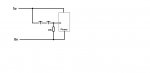
I am new to the picaxe 401 (28x2). I have been trying to build the circuit on page 78 of Manual #1. Since I am rusty on electronics the diagram does not show me enough information to build the circuit. I did change the code upon copy/paste to reflect the use of port A.0 as an analog rather than the C.1, but still no blinking LEDs when I shade and unshade the LDR. Some more info on how to wire it would be of help if someone can post it. I am using a mini breadboard which is mounted on top of a shield, if that is of any assistance.

Thanks,
Paul
 

eclectic

Moderator
Welcome to the Forum Paul.

I've moved your post to the Active Forum,
where it will get more exposure.

First quesion for you:
Can you post a hi-res photo of your setup,
so that folks can give you more advice?

e
 

Jamster

Senior Member
Welcome to the Forum,

It will help us to help you if you post a picture of your current setup so we can see if there are any wiring faults. Also what value LDR are you using?

An easy thing to try is to replace the 10K resistor with a 50K (or similar) potentiometer and try adjusting that to change the sensitivity.
Also prehaps add the line "sertxd(b0)" after the "readadc A.1, b0": this will send the value of the input to the program editor, you can see the value sent by pressing F8 to open the terminal in the PE.

Jamster
 

SAborn

Senior Member
Or add the word " Debug " after the readadc line of code, then you will see all the variable values, and i think its much better for this application then sertxd.

Just dont use debug in code that requires precise timing loops and dont leave it in your final working code.
 

nick12ab

Senior Member
Ensure that you have included the pull-down resistor on the download circuit and also the current-limiting resistors on the LEDs.

I am using a mini breadboard which is mounted on top of a shield, if that is of any assistance.
Are you using the PICAXE shield base?

Also prehaps add the line "sertxd(b0)" after the "readadc A.1, b0"
You'd need to do sertxd(#b0,32) in order to see the number and for it not to merge into the others.
 

nick12ab

Senior Member
If the analogue pin is the ONLY modification you've made then on the shield base this'll be your circuit:


If you have modified the LED pins, then check if the LEDs are connected to the pins affected by the bright red jumper links.
 
Last edited:

pagoglia

New Member
Thanks for all the good information. I do not have a picture yet as I have continued experimenting after my original post. I will assume uploading pictures is easy to do and am likely to go that route. To clarify I have a proto shield on top of the 401 shield base, and the mini breadboard on top of the proto shield. So all the ports line up well between the two. I will try wiring the circuit as nick12ab suggests in his diagram. I will point out that he shows 'red' jumpers in the opposite arrangement from what I have, on the shield base. I have not made any modifications to the LED pins on the shield base, so am thinking my jumpers are ok as those positions were part of the original assembly directions. But one never knows.....

Paul
Oneonta, New York USA
 

inglewoodpete

Senior Member
I will assume uploading pictures is easy to do and am likely to go that route.
If you want to practice/play/experiment with the forum's tools, go to the Sandbox. First, go to the Forum home page; sandbox link can be found near the bottom of the home page.
 

westaust55

Moderator
To upload diagrams, photos, pdf's and any other permissible file types as attachments,
while you have a post or edit window open, Click on the "Go Advanced" button at the bottom right of the post/edit window.
Then in the formatting toolbars, click on the paperclip icon/button towards the right end of the upper row of the formatting tools.
 

nick12ab

Senior Member
Or take a look at the attachment for visual instructions on how to attach.

The red jumpers on the AXE401 shield base select whether certain pins go to the programming socket or headers on the base - if they are in the download position then an LED on the associated shield base connection will not light.
 

Attachments

lewisg

Senior Member
I have been trying to build the circuit on page 78 of Manual #1. Since I am rusty on electronics the diagram does not show me enough information to build the circuit.
I see your problem.

The circuit diagram assumes you know the top line is V+ (in this case +5VDC) and the bottom line is ground. The unmarked line in the center goes to a analog to digital (in this example ADC on C.1) input on the PICAXE. The top rectangle is a light dependent resistor (LDR) and the bottom rectangle is a 10k ohm resistor. These two resistors make a voltage divider circuit to provide a varying voltage to the ADC input depending on the amount of light striking the LDR.

The convention of positive power rail on top and ground rail on the bottom is illustrated on page 7 of Manual #1 where the circuit of the LEDs for this program are diagrammed. This convention is also illustrated on page 79. I agree that placing three text labels on this drawing would have helped.
 

pagoglia

New Member
Well,I finally got this circuit working. I ended up using a pot to figure out the resistance needed for the fixed resisotor and am using a 15K. Works good and numerous bits of info from all of you helped to get me to this point. I am now building the circuit on page 77 where one can turn on a LED for 1 second each time a button is pushed. Got that to work as well. But, when I tried adding a second switch, so the two switches behave as an 'AND' gate, I am stuck. Looks like one side of each tactile momentary on switch should be wired to +5V and the other side of each switch to a respective Input. But that does not work. I'll play some more and maybe get to where I'll post a picture.
 

pagoglia

New Member
I understand how the diagram shows how to wire two switches in series to get and 'AND' effect. But how do you use the switches to monitor two port pins? For example say I want one switch on portC.1 and one on portC.2 what would the wiring look like? This is a variation suggested on page 77 of manual 1 and although I can get one switch to turn on the LED, when I modify the circuit to include a second switch and a second picaxe pin, the LED does not light when both switches are depressed. There is something simple I am missing!
:eek:
 

westaust55

Moderator
Okay, so if I interpret correctly, you know how to wire 1 switch to 1 input and that is working.
To add a second switch to another input, it is wired up in exactly the same manner.

Could it be that the difficulty is more how to program to monitor both switches/inputs and then control the LED or LEDs accordingly.

Tell us in simple steps / plain English how you want the switches to control the LEDs and someone will give you an e example.
Alternatively post your existing program Nd we can highlight where to change it.
 
Top