terrapinlogo
Member
I have a keypad and led display that I have pulled from an old house alarm and I am trying to get the display half going with a 20X2 (haven't tried the keypad half yet). But I am having no luck. I can clock the data in manually by connecting the clock and data lines to ground but I cannot get it to work with the 20X2. Here is the code that I have been trying:
I found the original code on this forum somewhere and then modified it for hspi and to transmit 16bits instead of 8
Code:
symbol clock = b.7		; clock on b.7
symbol pattern = w0     	; variable to hold the LED pattern
symbol delaytime = b15		;variable to hold the delay beetween changes

init: low clock				;Set up the chip and outputs etc
      pattern = %0000000000000001
      delaytime = 1
	hspisetup spimode11, spislow
	output b.7

main:								;Change the pattern then
	DO
		GOSUB out_595				;gosub to output the data
		pause delaytime
		pattern = pattern <<1
	loop until pattern=%1000000000000000
	DO
		GOSUB out_595
		pause delaytime
		pattern = pattern >>1
	loop until pattern=%0000000000000001
	goto main

out_595:			;transmit the data to the board
	hspiout (b1)
	hspiout (b0)
returnAttachments
-
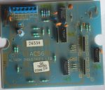
 303.5 KB Views: 20
 -
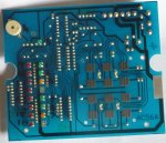
 228.8 KB Views: 24