westaust55
Moderator
The ideal interface between a PICAXE chip and an LCD display module is usually a 1-wire serial interface. This is done to:
- minimize the number of output pins required (essential on smaller PICAXE chips)
- utilize the inbuilt SEROUT command for ease of operation.
- achieve higher speeds in data transfer to the LCD module
Revolution Education (AXE033) and PH Anderson sell some very good examples of 1-wire based LCD displays
One downside of the 1-wire serial interface can be the cost associated with the serial interface board.
two frequent alternatives used by many are:
- the serial to 4-bit parallel FRM010 firmware chip sold by Revolution Education and presented in the PICAXE manual 3 on page 34
- the 6-wire interface as presented in PICAXE manual 3 on pages 35 to 39
This project offers a further alternative using either a 2 wire or 3-wire approach.
The 2-wire approach is generally best suited to the 08M and smaller PICAXE chips whereas the 3-wire approach which saves a few bytes of program code and is slightly faster is generally better suited to the mid to larger PIACXE chips.
The concept is based on an approach used by Myke Predko. Myke’s approach used a hex shift register and the 4-bit parallel to LCD data interface method.
The difference is that this project utilizes two 74HC4015 IC’s. These chips contain dual 4-bit shift registers giving a total of four 4-bit shift registers. Three such registers are linked in series as a 12 bit shift register which can handle:
- 8 parallel data bits to the LCD module
- the RS signal line
- the E signal line
- control bit for the backlight
The 12th bit is not used in this project.
The last 4-bit shift register is used to take the backlight control bit from the main shift register and latch that bit when the “E” signal is passed to the LCD module. This prevents the backlight flickering on and off when new data is being shifted into the 12-bit shift register.
The following posts provide:
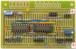
1. The shift register interface board layout PEBBLE files
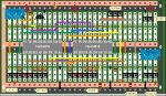
2. The shift register interface board schematic
3. The shift register interface board timing sequence
4. The PICAXE code with example text to control the LCD via the shift register interface board
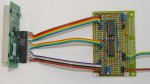
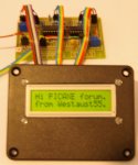
5. A few photos of the interface board etc
Attached below are the PEBBLE layout files
EDIT: Some further recommendations:
1. Not all LCD modules have onboard current limiting resistors. For those using an LCD module without such an inbuilt current limiting backlight resistor, I recommend to add say a 5.6 or 8.2 Ohm resistor in place of the orange wire at the very left of my layout diagram in Post 1.
2. The aim is to operate the LCD backlight switching transistor in saturation to minimise the Vce voltage. In place of the 4.7kOHm resistor I have used, to accommodate operation from a 4.5V (3xAA cell) supply, a 3.3kOhm resistor would be a better option (still acceptable at 5V).
- minimize the number of output pins required (essential on smaller PICAXE chips)
- utilize the inbuilt SEROUT command for ease of operation.
- achieve higher speeds in data transfer to the LCD module
Revolution Education (AXE033) and PH Anderson sell some very good examples of 1-wire based LCD displays
One downside of the 1-wire serial interface can be the cost associated with the serial interface board.
two frequent alternatives used by many are:
- the serial to 4-bit parallel FRM010 firmware chip sold by Revolution Education and presented in the PICAXE manual 3 on page 34
- the 6-wire interface as presented in PICAXE manual 3 on pages 35 to 39
This project offers a further alternative using either a 2 wire or 3-wire approach.
The 2-wire approach is generally best suited to the 08M and smaller PICAXE chips whereas the 3-wire approach which saves a few bytes of program code and is slightly faster is generally better suited to the mid to larger PIACXE chips.
The concept is based on an approach used by Myke Predko. Myke’s approach used a hex shift register and the 4-bit parallel to LCD data interface method.
The difference is that this project utilizes two 74HC4015 IC’s. These chips contain dual 4-bit shift registers giving a total of four 4-bit shift registers. Three such registers are linked in series as a 12 bit shift register which can handle:
- 8 parallel data bits to the LCD module
- the RS signal line
- the E signal line
- control bit for the backlight
The 12th bit is not used in this project.
The last 4-bit shift register is used to take the backlight control bit from the main shift register and latch that bit when the “E” signal is passed to the LCD module. This prevents the backlight flickering on and off when new data is being shifted into the 12-bit shift register.
The following posts provide:
1. The shift register interface board layout PEBBLE files
2. The shift register interface board schematic
3. The shift register interface board timing sequence
4. The PICAXE code with example text to control the LCD via the shift register interface board
5. A few photos of the interface board etc
Attached below are the PEBBLE layout files
EDIT: Some further recommendations:
1. Not all LCD modules have onboard current limiting resistors. For those using an LCD module without such an inbuilt current limiting backlight resistor, I recommend to add say a 5.6 or 8.2 Ohm resistor in place of the orange wire at the very left of my layout diagram in Post 1.
2. The aim is to operate the LCD backlight switching transistor in saturation to minimise the Vce voltage. In place of the 4.7kOHm resistor I have used, to accommodate operation from a 4.5V (3xAA cell) supply, a 3.3kOhm resistor would be a better option (still acceptable at 5V).
Attachments
-
 175.8 KB Views: 430
 -
4 KB Views: 174
Last edited: