The website says that the 14M2 datasheet is the PIC16F1825. But I see the 14M2 has ports C0-5 and B0-5, whereas the 1825 has ports C0-5 and A0-5 meaning that the pins are named differently and in different positions.
Then I looked at the 18M2 = PIC16F1847, and compared it to "PICaxe 18M2 SFR Data Ver_A.pdf" from here :- http://www.picaxeforum.co.uk/showthread.php?11514-PICAXE-Memory-Map-and-SFR-Details-Chart/page2 Post# 13. - nice chart.
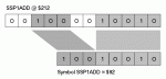
I notice that SFR locations differ ie. SSP1CON1 in the 1847 datasheet is at $215 but in the "PICaxe 18M2 SFR Data Ver_A.pdf" it is at $95.
So I am confused on several counts.
1. Why the different port/pin designations?
2. I don't understand SFR and cannot find out how correctly calculate the Bank# etc. ie. how did $215 become $95?
3. Is my coding attempt anywhere close?
I am interested in trying to use the hardware SPI port. Here is the code as of now. I suppose that I have learnt quite a bit doing this exercise, but it is coming to a frustrating ending. So any guidance and hints will be gratefully accepted.
Then I looked at the 18M2 = PIC16F1847, and compared it to "PICaxe 18M2 SFR Data Ver_A.pdf" from here :- http://www.picaxeforum.co.uk/showthread.php?11514-PICAXE-Memory-Map-and-SFR-Details-Chart/page2 Post# 13. - nice chart.
I notice that SFR locations differ ie. SSP1CON1 in the 1847 datasheet is at $215 but in the "PICaxe 18M2 SFR Data Ver_A.pdf" it is at $95.
So I am confused on several counts.
1. Why the different port/pin designations?
2. I don't understand SFR and cannot find out how correctly calculate the Bank# etc. ie. how did $215 become $95?
3. Is my coding attempt anywhere close?
I am interested in trying to use the hardware SPI port. Here is the code as of now. I suppose that I have learnt quite a bit doing this exercise, but it is coming to a frustrating ending. So any guidance and hints will be gratefully accepted.
Code:
' initialize the SPI module to have idle for clock low, send at middle of clock pules
' transmit on idle-active, use clock/64
' also needs to set the SS and SPI pins to proper outputs


' symbol OSCTUNE = $98
symbol SSP1BUF  = $91  ' or $211 ??
symbol SSP1STAT = $94 ' $214
symbol SSP1CON1 = $95 ' $215
symbol APFCON0  = $11D
symbol APFCON1  = $11E

symbol TRIS_A = $8C
symbol TRIS_C = $8E

Main:
	Gosub InitSPI
'	debug
	Gosub WriteToSPI
'	debug
	Goto main

InitSPI:
' B3 SCK0 output, B4 SDI input, B5 SDO output
		   '76543210
 let dirsB =	%11111111 	' set port pin directions
 ' let dirsC =	%11011111

 b1 = 0
 		pokesfr b1,SSP1CON1 	'turn off module, in case it was on
 		pokesfr b1,SSP1STAT		'send at middle of clock, transmit on idle->active
 b1 = %00100010
    pokesfr b1,SSP1CON1		'enable MSSP, idle is low,clock/64
 b1 = %0
'    pokesfr b1,APFCON1		'alternate pin config
 return


WriteToSPI:
     b1 = $55
     pokesfr b1,SSP1BUF
     pause 50
     return