Build a 14M based Logic Probe

westaust55

Moderator
In a previous life long ago, I had a home brew 5 state TTL logic probe for 5V supplied circuits but since resumption with electronics projects and PICAXE microcontrollers 3 years ago, test tools have been only a DMM, not that I have had any problems needing oscilloscopes, etc thus far.

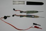
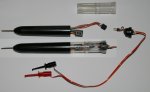
That said, I decided to create a new Logic Probe based on a 14M PICAXE chip.
Many simpler logic probes use two or three LEDs as the logic state display and a few use a 7-segment display to show “H” or “L”.

Considering that PICAXE chips are now available in lower voltages my logic probe has considered a nominal range of 3 Volts to 4.5 Volts and 5 Volts as the circuit supply voltage. Accordingly a simple form of automatic supply voltage level detection is included. The circuit voltage level detection uses the forward volt drop across a 1N914 diode as a rough voltage reference.

The logic probe can indicate 9 separate “states” or voltage levels as:
Code:
0)  <= ~ 0.10 V    then effectively at 0V rail  
1) <= ~ 0.15*Vdd and Vdd = 3 V then a TTL low state, or 
             if <= 0.8V at 4.5/5V then TTL low state (plus ST plus CMOS)
2) <= ~ 0.20*Vdd  then a Schmitt Trigger low state plus CMOS low state
3) <= ~ 0.266*Vdd then only a CMOS low state
4) > state (3) and < state (5) is logic indeterminate or tri-stated/high impedance  
5)  > ~ 0.25*Vdd+0.8V and Vdd = 3 V then TTL high state or
            if > 2.0 V at 4.5/5V then TTL high State
6)  > ~ 0.733*Vdd then also a CMOS high state (CMOS + TTL)  
7)  > ~ 0.8*Vdd   then also a Schmitt Trigger High plus TTL high plus CMOS high
8)  > Vdd - 0.2V then effectively at Vdd rail
While most of the time a &#8220;1&#8221; or &#8220;0&#8221; will be displayed, noting that occasional folks have had problems with for example, a lower voltage TTL acceptable level &#8220;high&#8221; signal onto a Schmitt Trigger (ST) input not working, having the differentiation for ST and CMOS may be warranted in some cases.

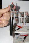
The circuit as posted is working well on a breadboard and I now about to assemble on a PCB and install into a 2cm diameter pen housing.

The 14M output 0 was deliberate not used to drive the 7-segment display and thus is available to allow interface to a terminal window should one wish to pass any status data on to a terminal screen. By way of example I pass the supply voltage as detected and with around 20 program bytes remaining a couple of extra variables could also be transferred if desired.

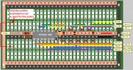
For those who are interested, the program listing is attached and embedded within the comments is a pseudo schematic with PICAXE 14M pin assignments.
Note for clarity the resistors for the programming circuit are omitted. :cool:
 

Attachments

Last edited:

BillyGreen1973

Senior Member
Thanks for sharing Westy.

Just a quick question, and I'm sure others will be thinking this too, but why the 'odd' displays on the 7 seg? Why not just display the '1', '2'...etc?
I'm sure there is a very simple answer, but its not 'hitting' me yet :rolleyes:

Thanks
 

westaust55

Moderator
Hi BillyG,

The reason for using the symbols was for (to me at least) quicker interpretation.

If you have not used it for a while, what does "state 4" mean without looking up a chart ?


If the LED at the top ("A" segment" is illuminated then the signal is near the top voltage available,
If the bottom LED ("D" segment) is illuminated then the signal is near the 0V supply rail.
If the middle ("G" segment) is illuminated then the signal is indeterminate between logic low and logic high.

A small "0" (o) suggest a low state acceptable to some types of logic whereas a full height "0" (O) suggests a low state acceptable to all logic types

A small "1" suggests a high state acceptable to some types of logic whereas a full height "1" suggests a high state acceptable to all logic types

CMOS has some different voltage levels again hence the "c" in the upper or lower half of the display.

Hope that gives some insight and makes sense.

It would be easy enough to change the symbolic patterns on the 7-Seg display if one so desired by reworking the 8 EEPROM data values.
 
Last edited:

charentemaster

New Member
different indicator

Yes good project but difficult to remember the corresponding
logic level, why not use a 'LED bar' display and then it would be simple
to remember position eg position 2 = xyz etc

cheers
 

westaust55

Moderator
It can all come down to a case of personal preference.

Size and perceived “readability” are my drivers for the format chosen and presented.

For size:
I can buy a 0.39 inch/9.9mm high 7-Segment display from Futurlec (overall dimensions 13 x 10 mm)
Alternatively, a DIL packaged, 10 segment, LED bargraph display from most sources have overall dimensions of 25.4 x 10 mm.
So on size, the 7-Seg display is half the height and thus better to fit into a large plastic pen type housing along with the other components.​

For readability:
The “symbolic” format I presented seems to me at least to be more easily readable from a quick glance at the display. Is that “1” / high state just a “1” or high enough to suit all logic types ?
See the attached sheet as an example. Which makes sense quickly to you?​


However, at the end of the day to use digits 0 through to 8, or a bargraph only requires the codes held in EEPROM to be changed. For a 10 segment bargraph, Options are to use only 7 or 8 segments or you will need few 1N914 or similar diodes to drive the full 10 segments from 7 PICAXE outputs (8 outputs if you do use Output 0).
 

Attachments

westaust55

Moderator
Here is a version of the 14M based logic probe.

The pen case was one of those 10-colour ball point types.
The wiring is a bit of a rats nest due to space limitations and use of through hole components but it fits and the clear upper part makes it easy to see the 7-seg display without cutting a hole.
Will soon use some clear silastic to fill the slotted holes in the clear upper part near the top.

The black plastic top "plug" is part of the orginal pen held in place with a small screw and the wires terminate on a 2x3 header socket. The 4 wires arranged so that reverse insertion of the external leads will do no damage. :)

For the 2x3 header sockets, I have one set of flying leads with the IC test clips for power connection and another lead which enables conenction of an AXE027 or other programming lead to download a program into the 14M.

I have in this pen based logic probe swapped the ADC inputs for the voltage reference and probe input for a better layout compared to the orginal breadboarded circuit as included in the program in Post 1.
 

Attachments

westaust55

Moderator
Here is a composite photo showing some of the 9 display states using a series of resistors between +Vcc and 0V to provide some intermediate voltage test points.

Works well across a range of volatges and some of the display states are with 3V for the supply and others with 5V with no difference on presentation.

Keep in mind that the 7-Seg display illuminated segments are a bit washed out due to the camera flash.

Will upload a schematic soon . . . . .
 

Attachments

Last edited:

westaust55

Moderator
14M based logic Probe layout

Attached are the data file and an image based on the layout as I created in PEBBLE.

I did create an initial version on strip board which did not provide the Vcc and 0V supply rails down the length of the board which made the board longer. The use of strip board with only 5 holes wide also involved the need to cut a number of tracks between holes to isolate parts of the circuit.
 

Attachments

westaust55

Moderator
Build a 14M based Logic Probe - Enhanced for Pulse train detection

Modified PICAXE program code now occupies 255 out of 256 bytes.
The added feature is that the display will not show a "P" on the 7-seg display if a pulse train of 8 Hz or greater is detected.
Code would save a few bytes by removing the data going back to the PC at start-up should one wish to further enhance the program.

Code:
;===============================================================================
; Program using a PICAXE 14M and 7-Segment display as a logic level probe
;
;
;                                    ____  ____
;  +Vcc ----------------------  +V -|    \/    |- 0V
;                                   |          |
;                                   |          |
;     Std Program cct here - SerIn -|          |- SerOut
;                                   |          |
;                                   |          |
;  +V - 1k0-+----- Vref on ADC4 In -|  PICAXE  |- LED 'A' 
;           |                       |          |
;         | |                       |          |
;          ---          Unused In3 -|   14M    |- LED 'B'
;          / \ 2.4V Zener           |          |
;          ---                      |          |
;           |           LED 'G' C5 -|          |- LED 'C'      
;          0V                       |          |
;                                   |          |
;                       LED 'F' C4 -|          |- LED 'D'
;  +V - 10M-+                       |          |
;           |                       |          |
; Probe-----+---------------ADC0In -|          |- LED 'E'
;           |                       +----------+
;          4M7 
;           |
;          0V
;
;
;

;
;
;  PICAXE pins via 620 Ohm resisitors to all 7-Seg display segments. dp via 1k0 Ohm to Vdd as 'On' indicator.
;
;  Programming circuit resistors not shown for clarity.
;
;  Potential divider using 10M and 4M7 resistors holds the probe pin in an indeterminate state when no signal present.
;
;  1k0 resistor in series with 2.4V zener diode as simple ref voltage to detect Vdd level (3, 4.5 or 5 Volts)
;
; Definition of (state) if signal at probe is:
; (0) <= ~ 0.10 V    then effectively at 0V rail  
; (1) <= ~ 0.15*Vdd and Vdd = 3 V then a TTL low state, or if <= 0.8V at 4.5/5V then TTL low state (plus ST plus CMOS)
; (2) <= ~ 0.20*Vdd  then a Schmitt Trigger low state plus CMOS low state
; (3) <= ~ 0.266*Vdd then only a CMOS low state
; (4) > state (3) and < state (5) is logic indeterminate or tri-stated/high impedance  
; (5)  > ~ 0.25*Vdd+0.8V and Vdd = 3 V then TTL high state of if > 2.0 V at 4.5/5V then TTL high State
; (6)  > ~ 0.733*Vdd then also a CMOS high state (CMOS + TTL)  
; (7)  > ~ 0.8*Vdd   then also a Schmitt Trigger High plus TTL high plus CMOS high
; (8)  > Vdd - 0.2V then effectively at Vdd rail  
; (9) If there are pulses are greater than a pre defined frequency (typcally 8 Hz) then the display indicate "P"
;
;
; 7 Segment display images for states 0 to 9
;   (0)    (1)    (2)    (3)    (4)    (5)    (6)    (7)    (8)   (9)
;
;   . .    ._.    ._.    . .    . .    . .    ._.    . .    ._.   ._.
;          | |    | |                         |        |          | | 
;   . .    . .    .-.    .-.    .-.    . .    .-.    . .    . .   .-.
;          | |           |               |      |      |          |
;   .-.    .-.    .-.    .-.    . .    . .    . .    . .    . .   . .
;
;
;
#PICAXE 14M
EEPROM 0, (%00010000, %01111110, %11000110, %10110000, %10000000,%00001000,%11001010, %00001100,%00000010,%11100110)

SYMBOL LED	  = b0    ; Bit code from EEPROM to set the 7-Segment display for current signal logic state
SYMBOL Vref   = b1    ; Reference Voltage read by ADC from 2.4V zener voltage
SYMBOL Logic  = b2    ; Circuit Signal Voltage 
SYMBOL Vss    = b3    ; Supply voltage x 10
SYMBOL State  = b4    ; state for the current signal logic level
SYMBOL Prev   = b5    ; Used to hold a previous logic state
SYMBOL Temp   = b6    ; Temporary variable
SYMBOL Spare1 = b7
SYMBOL Spare2 = b8
SYMBOL Spare3 = b9
SYMBOL Spare4 = b10
SYMBOL Spare5 = b11
SYMBOL PlsChk = w6    ; w6 = b13:b12

SYMBOL PlsDur   = 1000 ; pulse check duration - 1000 = 500ms at 8MHz
SYMBOL Min4pls  = 4   ; minimum number of pulses in the pulse duration before a pulse train is deemed to exist

SYMBOL RefPin   = 4   ; input 0 as ADC for reference voltage
SYMBOL ProbePin = 0   ; input 4 as ADC for the signal being monitored

#TERMINAL 9600
; ===============================================================================
;Initialiseation - here we identify the circuit supply voltage as a reference for
;determination of the various voltage levels
; 
Init:
	
	SETFREQ m8
	PAUSE 1000 ; wait for 1 second for Programming Editor Terminal Window to initialise
	Prev = 9	; set an invalid state so always updates the display on the first pass after power-up.
	READADC RefPin, Vref
	SERTXD (#Vref, "  " )
	Vss = 50
	IF Vref >= 150 THEN
		Vss = 30
	ELSE IF Vref >= 130 THEN
		Vss = 45
	ENDIF
	Prev = Vss /10
	Temp = Vss // 10
	SERTXD (#Prev, ".", #Temp, " Volts.", CR, LF)
; ===============================================================================
; Main program loop to read the signal and determine the logic level.
;
Main:
	READADC ProbePin, Logic	; read the signal voltage level from circuit under test
	
	State = 8						; set as tied to Vdd rail by default,
								; then test if
	IF Logic <= 10  THEN 				; <= ~ 0.1 volts = direct to 0V rail ==> "_"
		State = 0
	ELSEIF Logic <=  40 AND Vss = 30 THEN	; <= 0.15*Vdd with 3 V supply = TTL Low 
		State = 1
	ELSEIF Logic <=  43 AND Vss = 50 THEN	; <= 0.80 V with 5.0 V supply = TTL Low
		State = 1
	ELSEIF Logic <=  47 AND Vss = 45 THEN	; <= 0.80 V with 4.5 V supply = TTL Low
		State = 1
	ELSEIF Logic <=  57 THEN			; <= 0.20*Vdd at any voltage for Schmitt Trigger Low
		State = 2
	ELSEIF Logic <=  70 THEN			; <= 0.266*Vdd at any voltage for CMOS Low
		State = 3
	ELSEIF Logic <=  99 AND Vss = 50 THEN	; <= 2.0V at 5.0 V supply (for min high state) = indeterminate
		State = 4
	ELSEIF Logic <= 108 AND Vss = 45 THEN	; <= 2.0V at 4.5 V supply (for min high state) = indeterminate
		State = 4
	ELSEIF Logic <= 130 AND Vss = 30 THEN	; <= 0.25*Vdd+0.8V at 3V (for min high state) = indeterminate
		State = 4	
	ELSEIF Logic <= 185 THEN			; < = ~0.733*Vdd at any voltage for CMOS High = high for TTL only
		State = 5
	ELSEIF Logic <= 202 THEN			; <= 0.80*Vdd at any voltage = high for TTL and CMOS
		State = 6
	ELSEIF Logic <= 240 THEN			; <= Vdd-0.2V at any voltage = high for Schmitt Trigger, TTL and CMOS 
		State = 7
	ENDIF
	
	COUNT ProbePin, PlsDur, PlsChk
	IF PlsChk > Min4pls THEN
	  State = 9                               ; A pulse train has bee detected 
	ENDIF
	 
	IF State = Prev THEN Main			; return now as no need to update the LED display
	
	READ State, LED
	OUTPINS = LED AND %00111110 			; Set up 7-segment parts A, B, C, D and E
	IF bit6 = 1 THEN
		HIGH PortC 4				; Set up 7-Segment parts F
	ELSE
		LOW  PortC 4
	ENDIF
	IF bit7 = 1 THEN
		HIGH PortC 5				; Set up 7-Segment parts G
	ELSE
		LOW  PortC 5
	ENDIF
	Prev = State
	GOTO Main
 
Last edited:

westaust55

Moderator
GASP......do we have to do everything around here?!?!?!??? :eek:

Thanks for that WA. Appreciated.
Hope you find it useful.

Re the decoupling caps . . .
When I go trolling the web at times and see sites where folks have posted a project with just a video or photo and some abstract be it on U-tube or another forum, it is amazing how many time the OP gets requests for the circuit scheamtic diagram, full program code, etc because the "requestor" wants it all for free :eek: to use for their secondary/tertiary education project :rolleyes:
So though I could leave something small for such freebie seeking folks to sort out for themselves ;)
 

Paix

Senior Member
If it's worth having, it's certainly got to be worth working for.

Students need to appreciate that an excessive leg-up is akin to cheating. They get the marks, but lack the smarts. Great on paper, but these things come back to bite people when later on they aren't able to understand the underlying principles.

Assistance is good, indeed often essential, but project work is project work for a reason and lazy students are apt to reap what they sow in the long term. best to get the smarts started while the grey matter is young and fresh.
 
Top