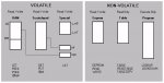
Hairy Animal
Member
I've been trying, with only partial success, to understand the M2 series devices' memory maps, and in particular exactly where various commands such as "TABLE" and "WRITE" actually write their data, so that I don't risk over-writing things.
I've looked at various threads on this forum (14M2 TABLE data is particularly useful and interesting) as well as the descriptions of the commands, but the more I look the more confused I get!
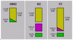
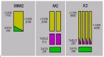
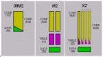
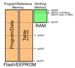
Based on the tables shown in PICAXE Chip Sizes, I've drawn up this simple diagram which, on the face of it, should represent the --M2 chips .....
However, when reading the "TABLE" command details, it states
Another point from the aforementioned thread; are flash and EEPROM memory just different names for the same type of memory having the same read/write speed etc?
What I find a bit confusing is exactly where commands such as "EEPROM" will actually write to. If I understand correctly, up to 256 bytes can be written as "EEPROM 0, byte1,..." etc and this will write to the main program flash memory starting at location &7FF and filling in the memory by decrementing from the top. Is this correct? Note, I presume this is case from the comment on the above page saying:
The other associated command is "WRITE". The description again doesn't make it at all clear (to me) where the command "WRITE 0, byte1,..." actually puts the bytes/words in the program/data memory. In particular, I'm worrying about a large program approaching 1792 bytes of code getting overwritten by data generated when the program runs? If the code takes 1792 bytes and all 256 spare bytes are written using EEPROM, is there any space left for WRITE data?
Apologies if the information I'm looking for (especially a memory map diagram) is available somewhere, but if it is I haven't managed to find it.
I've looked at various threads on this forum (14M2 TABLE data is particularly useful and interesting) as well as the descriptions of the commands, but the more I look the more confused I get!
Based on the tables shown in PICAXE Chip Sizes, I've drawn up this simple diagram which, on the face of it, should represent the --M2 chips .....
However, when reading the "TABLE" command details, it states
This would seem to conflict with the description of the M2 chips (except the 8M2) having a separate 2048 byte flash/EEPROM memory?M2 parts have 512 locations (0-511).
These are separate to the 2048 bytes of program memory, so do not affect program length.
Another point from the aforementioned thread; are flash and EEPROM memory just different names for the same type of memory having the same read/write speed etc?
What I find a bit confusing is exactly where commands such as "EEPROM" will actually write to. If I understand correctly, up to 256 bytes can be written as "EEPROM 0, byte1,..." etc and this will write to the main program flash memory starting at location &7FF and filling in the memory by decrementing from the top. Is this correct? Note, I presume this is case from the comment on the above page saying:
Then there's the table memory command. Superficially it looks much the same as the eeprom command. I presume that "TABLE 0, byte1,..." writes to the second block of flash memory starting at &000? But if only 512 bytes can be written with the "TABLE" command, is the rest of the 2nd block of 2048 bytes wasted?Program 1792 up to 2048 is EEPROM 255 to 0
The other associated command is "WRITE". The description again doesn't make it at all clear (to me) where the command "WRITE 0, byte1,..." actually puts the bytes/words in the program/data memory. In particular, I'm worrying about a large program approaching 1792 bytes of code getting overwritten by data generated when the program runs? If the code takes 1792 bytes and all 256 spare bytes are written using EEPROM, is there any space left for WRITE data?
Apologies if the information I'm looking for (especially a memory map diagram) is available somewhere, but if it is I haven't managed to find it.