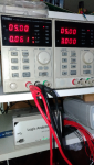
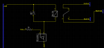
Yes i have a PSU. My PSU os in attach. I will try with 3 AA batteries and post here the result. Do you see my schema?
Hello Manuel
That PSU looks fine. I have heard of the brand but not used it. I am sure that being a Lab PSU it would have a clean output. I was just concerned that you might have been using a crappy SMPS plug pack or something of that nature.
I hadn't looked at your schematic until now. I noticed that on the Serial In connection, the 10k to Ground doesn't "look" quite right in terms of my experience with schematic capture software. As it is pictured, it doesn't look centered on the node. With my experience that can (sometimes) mean that although it looks connected, it isn't actually correctly connected to that node and could even be "floating". Depending on your PCB layout software, if it has DRC (Design Rule Check) and you didn't carry out a DRC, then something like this could be missed and carry over to the layout.
I looked at your layout, and although I think it looks right, if I were you, I would carry out the following steps (with POWER OFF to your project);
* Use a good quality DMM (Digital Multi Meter) and on the ohms scale (not continuity) put one probe on the Ground of your PSU (at the PSU end) and then probe around the Ground connection/s to the PICaxe and programming port. Obviously you are looking for near zero ohms.
* If you have a microscope, look at all of your SMD connections including ALL of the Pins on the PICaxe.
Another thing, what PCB layout software did you use? I'm no Engineering Guru, but, I'm fairly certain that vias (through holes) are a bit of a "no no" when placed in the middle of an SMD pad. A DRC would have likely flagged this as an issue. It might look good and efficient, but when you install the SMD component, you might accidentally fry your connection from one layer to the next. So with that in mind, I would check for very low ohms along ALL of the tracks from the programming port to the Serial Out, and from the programming port to the first resister, then from the other side of the 22k resistor to Serial In. From memory, you had at least one via in the middle of a pad on at least one of the resistors in the programming port arrangement. Basically check EVERYTHING (again if need be).
The only time I have ever come across vias in pads is when there were MANY put on a large pad and then they connected to another large pad on the other side. This was being used as a heatsink. Even if one of the vias got damaged, there were dozens involved so that ensured some degree of connection (albeit for heat as opposed to electronic connection).
Also, depending on who manufactured your board, some manufacturers will do a "bare board electrical connection check" which verifies the integrity of the PCB, whereas other might not carry out this test, meaning that small breaks in tracks (either due to manufacturing issues or design errors) or vias that look o.k. but fail to conduct from one side to the other might actually exist on your PCB. I wouldn't assume your PCB is o.k. You really need to double check it.
Let us know how you go.
Regards
Brad

") ) but I brainlessly hooked up the power backwards to a few in short times and they keep working fine
) but I brainlessly hooked up the power backwards to a few in short times and they keep working fine