Pebble

alanf

New Member
Hello

I am using Pebble, and like it very much with the slight reservation that saving and loading a display takes some time getting used to. Is the author still known as WestAust55? Has the program been upgraded/had its name changed and if so where will I find it? I may be pulled kicking and screaming into Windows 10 (I currently use Windows 7) or I may go to to Linux. Does the program work on either?
 

westaust55

Moderator
PEBBLE will work with Windows 10 - I am using it with Mozilla firefox for my PCB layouts including PICAXE based model railway DCC accessory decoder and accessory device control CAB for NCE based DCC systems which have been posted on this forum in the completed projects section.

I have not done any upgrade work for several years (due to first building a new house first and then heavy paying work commitment with long hours each day which helped pay off the new house). The version available for download from PICAXE.com should still be the latest.
Now free of the heavy work commitments since Jan16 but have not considered any further work on PEBBLE as yet.
 

OC71

New Member
It does work on windows 10. I am using it currently. BTW westaust55, thanks, It is a great app.
 

AllyCat

Senior Member
Hi,

but have not considered any further work on PEBBLE as yet.
Yes, it's an excellent application which I use quite a lot. It would be great if you could spend a little time on an update, or a small amount of documentation on how to add components (I have to confess that I'm not at all proficient with Java).

I have added about 20 components for my own use, but only in the "Misc" category, as described by wainon in post #733. They work well but often have an inconveniently large "hot" (active) area, making it difficult to select the correct component when moving them around.

The reason that I introduced some "new" symbols is that I like to use a "pseudo PCB" prototype construction method which I've been using for almost 50 years. It can employ either bare "perfboard" or "Veroboard" stripboard; the latter has the advantage of "anchoring" the components onto the board, but may involve a lot of track cutting with my very "compact" layouts. The principle is that if a through-hole component wire goes though an insulated hole (perfboard or a spot-face cut in Veroboard, then it can be "folded over" to connect with any of the 8 adjacent holes (and potentially some further away).

So I created a "spot face cutter" hole and four "BTC" (Bare Tinned Copper) wire symbols going N-S, E-W, NE-SW and NW-SE. That works very well, but would be even more convenient if one could just "drop" a spot cutter "hole" with a wire going to any of the 8 (or more) compass points. I also created a "CUT" symbol to use between holes to permit more compact arrangements. Physically it's very easy to do, just make two cuts in the track witrh a craft knife / scalpel and "pop-off" the intervening copper with a hot soldering iron.

Compactness has been important because I'm building circuits that are the size of a single AA battery (to use rather like a "placeholder" cell). The positive contact of the cell is emulated by a 3 or 4 mm pan-head bolt (6mm long) and the negative "base" by a solder tag / washer or just a loop of BTC. It's even possible to use the standard 3.5mm programming socket by standing it upright across one end of the board. The flat "pins" locate between the tracks so fillets of solder anchor them to all six tracks. The board is only 6 tracks wide (14mm) so smaller than Pebble offers, but that is not really an issue because it's useful to show the component and solder sides separately side-by-side.

Here's an example using some of the new symbols. It's not a board I've actually built / tested yet, but is basically an 08M2 which could monitor (on C.4) the current flowing in the (10 ohm) placeholder resistance and (for example) disable the series FET (driven from C.1) if the current gets too high or the voltage (measured via CALIBADC) or chip temperature are out of the desired range. "Diagnostics" data can be streamed via the programming port (or the chip reprogrammed) whilst in situ.

AAPlaceholderDemo.png

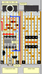
ADDENDUM: Note that the circuit as (still) shown above probably won't function as described/intended. The FET needs to control the current flow in the "base" connection of the dummy battery, not the tip. I have revised the layout (but still not tested), which also has some other potential advantages. The Weak Pullup resistor of the "input only" pin may control the FET, leaving both the "I2C" pins (C.1 and C.2) available for any desired purpose. Ask if you want to see the new arrangement.

Cheers, Alan.
 
Last edited:

westaust55

Moderator
Hello Allycat (alan),
I have just sent you a PM. If you send me the images you have created which will save me some time, I will look to adding them into PEBBLE along with an added proto-board and some spring terminals that I have been using.

Also, if anyone else has some parts/components they might like to have added then post the details here in the next few days and I will incorporate into one new update.
 

AllyCat

Senior Member
Hi,

It's a little disappointing that there has been so little feedback or suggestions, but it does seem rather "quiet" on the forum at the moment; of course it's the holiday season here in the UK.

I feel I've had more than my fair share of suggestions adopted, but here is some food for thought. A significant number of us still seem to use (sometimes) a three-pin header instead of the "official" 3.5mm jack for the "Programming" interface. The interface is SO useful, not just for In-Circuit Programming but for debugging and program development (using the DEBUG or SERTXD/SERRXD commands, etc.) that IMHO it should be included in all board designs. But the 3.5mm socket "blocks" 25 - 30 stripboard holes and even my vertical alternative (in #4 above) requires 15 - 24 holes (depending on its exact alignment), so it's easy to see why some people omit it. A Pin Header covers only 3 - 6 holes, depending whether any "polarisation" method is used (to prevent incorrect insertion).

However, the "Legacy" Programming Socket (3 pins with a "lock") is no longer included in Pebble. Of course it's possible to use the equivalent 3-pin "Locking Header" (white), but this has a few limitations: It doesn't have the Programming pin names marked, so I had to search quite deeply into an old .PDF version of Manual 1 to find them. Also, although the vertical "Lock" section looks quite clear in the .GIF images, it hardly shows in the overall PEBBLE view on (my) PC screen, and the pins in the inverted version (lock upwards) don't align perfectly with the stripboard holes. But do others use the Legacy socket as such, or just fit an "arbitrary" pin header (which is still far better than nothing) ?


Secondly, has anybody used the ebay "Veroboard Stripboards" that are neither stripbords nor made by Vero ? You may know that I've recently been designing small prototype boards which require a large number of cuts in the copper strips to isolate sections of track. Then, the adhesion of the copper to the "Paxolin" (paper + epoxy) base material can become rather poor. So I've been looking for alternatives and found several listings like this example. Note that it is not actually stripboard (and certainly not manufactured by Vero) but it does look to be of good quality, being glass fibre with pads on both sides and plated through holes. There are a number of standard sizes but the 5 x 7 cms (18 x 24 holes) particularly interests me; I could cut 3 or 4 of my "AA cell" sized boards from each, and 5 boards can cost less than $2 from China. But I will have to be patient because locally-sourced they cost almost ten times as much. :(

So has anybody used them, and how? I guess they were originally intended for wire-wrap sockets, but how to design for them in a "PCB" form? In principle one can use the standard "Stripboard" in Pebble and ignore the copper strips, but I do find my "mindset" very much assumes that vertical conductors are present. So perhaps just design the board as if the vertical tracks are there and then add wires where they're actually needed as a final stage? Also, I do foresee two disadvantages with boards of that type: it can be much more difficult to remove/change components in PTH boards, and cutting the Fibreglass destroys files and drill bits very rapidly. :(

Cheers, Alan.
 
Top