315 wireless/PICAXE controlled LED circuit.

clonetwo

New Member
Hi, I'm new to this forum and I have some questions about a project I'm working on.

If anyone can help me with setting up a PICAXE 08M2 transistor and relay I be very happy :)

I have been working on this project for awhile now in my spare time and I have almost completed the project, but I'm lacking is a few skill and hope I can find help here!

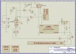
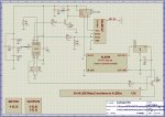
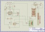
Ill post a circuit diagram for review and if anyone has questions or comments please reply.


I have a PICAXE 08M2 and the power supply is a 1.5 or 1.2 volt 3 cell pack..

I have a basic wireless module like this http://www.ebay.com/itm/315Mhz-WL-RF-transmitter-Receiver-Module-Link-Kit-for-Arduino-ARM-MCU-Wireless-/400479296104

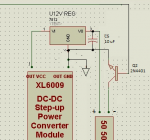
I have this DC/DC Boost converter. http://www.ebay.com/itm/DC-DC-Adjustable-Step-up-boost-Power-Converter-Module-XL6009-Replace-LM2577-/310717070508?pt=LH_DefaultDomain_0&hash=item48582e3cac

The CD/CD boots converter is for powering 12V LEDS I have 3 segments from a 50/50 LED strip ( That is 9 LEDS total )

and I have a 5volt relay to redirect power the dc/dc boost

Now I'm using a transistor type 2N4401 to turn on the relay from the PICAXE 08M2
and another 2N4401 to blink the led controlled from the PICAXE 08M2 as well.

Picture2.jpg

I need to know (because i'm a nube and this is pretty much my first project of many to come :D),

1. I want to make sure I have correct resisters on unused PICAXE pins for battery efficiency.
2. What kind of relay should I use?
3. What type of transistors should I use.
4. Where should I have resisters (should I have some on LED or on the DC/DC boost or on the transistors, ect)
5. any other tips/insight.

I think if these answers are found I would be well on my way.
Thanks and regards,
CloneTwo
 
Last edited:

BeanieBots

Moderator
Hi and welcome to the forum.
Please remember that people give their time for free so provide as much information as possible.
I for one do not have the time to convert your layout into a circuit diagram so please post the circuit so that people do not have to do lots of work up front.
 

clonetwo

New Member
updated the picture.

OK, i have updated the picture. i used my new copy of PICAXE VSM!!! :p

thanks guys, i hope this did not get pushed to far down the forum.

Regards,
Clonetwo
 

BeanieBots

Moderator
Hmm... Much better but I still have great difficulty following your diagram!
For instance, it is not obvious where or what is your 0v line.
As a guide, a circuit should flow with signals going from left to right and current (conventional) from top to bottom.
I usually start with two parallel lines, one at the top for power and one at the bottom for 0v.
Then put all the inputs on the left, all the outputs on the right and then fill in the rest.

It's like normal writting. Sentances, punctuation and paragraphs.. left to right, top to bottom.
Anything other than that and it would be very hard to read.
Don't forget, we have no idea about your design and despite popular beleif, we cannot mind read either.
Hopefully somebody will be along soon to help you out. I'll try a bit later when I have some more time.
 

Goeytex

Senior Member
Q2 will not work as drawn. As an NPN it should be a low side switch. See the suggested change below.

Also consider using ground symbols instead of snaking the ground line all over the diagram. While not a hard rule, it is common practice to have the emitter of a NPN transistor pointing downward.
 

Attachments

Last edited:

Bill.b

Senior Member
Both VCC and Ground are connected to the same point via the relay.

The VCC connection on the step up module and the RF module should be connected to the Positive terminal of the battery.


Bill
 

clonetwo

New Member
Both VCC and Ground are connected to the same point via the relay.

The VCC connection on the step up module and the RF module should be connected to the Positive terminal of the battery.


Bill
YES! your right Bill! totally goofed that part. I can assure you that is not how it is on my prototype project board :eek:

ok, I'll remake the schematic using the ideas BeanieBots gave. will re-post new schematic soon.

I will also add a connection to ground as Goeytex suggested though it seemed to work with out, I think it will be better to have ground there.

Thanks!
CloneTwo
 

BeanieBots

Moderator
I will also add a connection to ground as Goeytex suggested though it seemed to work with out, I think it will be better to have ground there.
I don't think that is what Goeytex meant. I think he was suggesting that you use ground symbols in your diagram rather than trying to show all the ground wires on the diagram. I do not beleive he was suggesting making a connection to 'ground' (earth).

Personally, unless the diagram is large and complex, I prefer to show the actual connections and where possible, the ACTUAL point of contact but that's because I'm predominantly working with analogue where it is important WHERE on the 0v line a particular connection is made.

The other point that Goeytex made was about the transistor orientation. However, if you stick to the basic guidlines of flow from top to bottom, your transitor will automatically be the right way around. If not, then you may well have made a mistake. It's not 100% failsafe but all these conventions do actually help to sanitise the design (it simply looks wrong if it is wrong) but it really does make it much easier to follow and spot errors.
 

fernando_g

Senior Member
It appears that you are powering up and down some boards with a relay that switches the ground (return)....this is not a good idea. Switch the Vcc (battery) supply, always.
 

rq3

Senior Member
It appears that you are powering up and down some boards with a relay that switches the ground (return)....this is not a good idea. Switch the Vcc (battery) supply, always.
Oddly, this is very common in aircraft wiring, for absolutely no good reason. Mooney and Beechcraft commonly "lift ground" to control ancillary functions (like lights), and it makes troubleshooting insane. You can imagine the quantity of steering diodes it takes to do this in an airplane, and each diode must take the full load being controlled!

And in an aircraft, weight is everything. There must be, conservatively, 15 pounds of circuit boards (with diodes, resistors, transistors) in a typical Beech Bonanza to control simple circuits that could have been more safely controlled with just an SPST switch.

I suspect this an example of "feature growth". Rather than start over and do it right, they patch in new stuff and try to get it to co-operate with existing crap. Sometimes (oft-times) it's best to clear the slate and start over!
 

clonetwo

New Member
Okay, I have re done the schematic, I fixed three errors, including relay now switches Vcc instead of ground. I would never had know that its bad on ground so that tip help a ton.
also I fixed the NPN on the 12v power converter. once I saw how I drew that... :mad:

BeanieBots, can you let me know if my schematic is easier to read?, I miss understood inputs and outputs in this one to. so I added a key at the bottom instead of redrawing it again.

Picture5.jpg
The PICAXE VSM software is nice! Three thumbs up!!

If there is any weird or of question components, lacking or otherwise please tell so I can make corrections.

Thanks for the help again.
Regards,
clonetwo
 
Last edited:

Goeytex

Senior Member
It looks much better.

1) If you are not going to program the Picaxe in circuit, then R2 can be eliminated. A single 10K is fine.

2) Assuming the RF device is a receiver and the data is an input to the Picaxe, then R4/R5 are forming a voltage divider and will reduce the signal level to the Picaxe. TO correct this, place R5 on the other side of R4.

3) The RF device shows no external antenna. It should also be clearly labeled as a receiver.
 

clonetwo

New Member
OK i have made those adjustments.

Picture6.jpg

Thanks so much for the help.
this really makes me feel much better about my project!

I plan on sticking around and learning more!!

Regards,
Clonetwo
 
Top