I'm interested in "packaging techniques" and soldering breadboards that don't have land patterns. Are you aware of reference documents that would show packaging techniques, and using pattern-less boards? I'd appreciate any links that you will share. Thank you,
Jims
Sorry for the delay, not been here for a while.
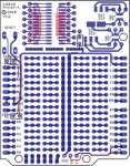
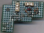
I attach a scan of a board i recently made to upgrade a customers device.
Space was very limited and some components need to be at other side, some here...
Larger photo: Down at right there are two SOT23 3 pin devices, and between them a SOT323.
They are easily laid out like i had drawn the solution on a piece of paper.
The SOT23 are "microcontroller reset IC:s" but they are here used for checking and sequencing power. (they have good voltage ref, shmidt-trigger comparator and delay inside, and push-pull out. Pretty much for a buc and three pin soldering
")
. Also simple FET like 2N7000 or similar often save a resistor. sometimes the "digital transistors" (NPN or PNP plus one or two R ina SOT23 or SOT323 package) is even better as they do not need pull down. There is a much larger range of components avaialble as SMT than through-hole.
Easy to solder: fill a hole with tin, grab the component with a plier and put it to that tin while melting it again.
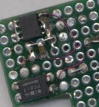
On the other side are some 0603 and 0805, they easily fit between two pads. The SO8 is a FET with only 6 milliohms R. It is most ofte a good idea to use "over sized" semicondictors so they are cooler, so overall size and cost incl work actually get lower, plus more dobust.
The thin wires are enamelled wires of a type that the enamel melts when soldering to the end. Very convenient.
Routing, rerouting, and high signal density is easy wuth these.
If you need tens of amperes, use large wires, and also in this case it beats etched designs easily. (for one offs opr a few that is...)
On through plated boards I often mount "through-hole components" like SMT too - not sticking them through board holes make it much easier to change value or completely alter the design.
______________________
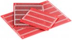
However, inspired by seeing other protoboards in this thread i went shopping:
http://www.ebay.com/cln/morganlej/Protoboards/96229069011
I especially like this one currently top left on the link i gave:
http://www.ebay.com/itm/5x-Proto-PCB-69-x-50mm-w-452-Pad-SMT-Green-5pcs/331153410014?hash=item4d1a4807de
because in a very efficient way you can mount either DIL or SOIC or SOT23-3 on the same spot, plus it have hole triples connected to those connections, plus power strips.
And decent price. I just wish it had better provision for screw connections, but it is easy to drill between each 2 holes. But note this board is only 1 mm thick, so use one-peace blocks of many poles.
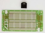
I also like this
http://www.conrad.biz/ce/de/product/531381 1,27 + 2,54 raster. Despite the high cost i like itbecause the holes are pretty big so the 1,27 mm raster area accept normal small through hole components like 1/8 W resistors, TO92 etc, and the 2,54 raster accept screw connectors. The one i recieved is 1 mm thick, not 0,7 as the catalog say.
One last tip: 3,5 mm spaced screw and jackable screw conectors suit diagonally a 2,54 mm raster.