PCBs

MikeGyver

Senior Member
1. print off artwork using a laser printer (Brother brand doesn't work). You want to use the thinnest, least absorbent paper you can find. Glossy magazine paper is clay based and will not absorb the toner. Since I don't have a printer, i've been using lightweight gloss paper from a fedex office 24hour print center, with excellent results.
1. scrub the copper with Scotchbrite 7447 pad until it is completely clean, bare copper. (no, don't use steel wool. we don't want to rub steel into the copper... 7447 is aluminum oxide)
2. clean copper with rubbing alcohol until paper napkin/towell is clean
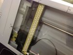
3. use a hot laminator to fuse the toner to the copper, run it through like 10 times (no, not 3). If you don't have a laminator don't waste your time by reading further. I use one of these and got it for $30 shipped http://www.google.com/products/catalog?q=gbc+9+creative+laminator&hl=en&safe=off&prmd=imvns&bav=on.2,or.r_gc.r_pw.r_qf.,cf.osb&biw=1228&bih=810&um=1&ie=UTF-8&tbm=shop&cid=16159181314241537830&sa=X&ei=bW6FT96LFqml8AGCvsCUCA&ved=0CG0Q8wIwAw
4. soak in water for a few minutes to help release the paper. You might have to scrub the paper with your fingers to get all the pulp off, don't worry, the toner isn't going to come off.
5. I lightly scrub the remainig pulp off using the scotchbrite pad to get down to the toner, I do this because I laminate Green TRF foil onto the toner to completely seal it. This only needs like 4 passes through the laminator.
6. lightly scub the board with the scotchbrite to remove any traces of un-bonded green TRF foil.
7. touch up any areas that require it using a sharpie permanent marker.
8. etch. I use muratic acid (31%) and hydrogen peroxide. 50/50 mix or slightly more peroxide than acid.
9. agitate while etching. if you just let it sit there it's going to take forever and your resist will deteriorate. you want to etch as quickly as possible. I use a sponge paintbrush and repeatedly wipe the copper very gently. This exposes new copper with each swipe and will etch the board in 5 minutes or less.
10. remove resist with acetone or brake cleaner, and give it a final scrub with scotchbrite to really clean the copper.
11. drill holes

I may have missed something... feel free to alter or add anything but you may get worse results.
 
Last edited:

clockwork

Member
Whilst on this subject I have nearly finished building a UV LED light box using cheapish LEDs purchased on the Internet, I have 60 LEDs (10 x 6 rows) 15mm apart and around 90mm from the PCB to be exposed. Can anybody give me the sort of time it would take to correctly expose the PCB. This will allow me to start testing times of exposure somewhere near the correct time. The PCB Board I have is the economy version sold by Tech Supplies of course.

Clockwork
 

MartinM57

Moderator
I have 60 LEDs (10 x 6 rows) 15mm apart and around 90mm from the PCB to be exposed. Can anybody give me the sort of time it would take to correctly expose the PCB. This will allow me to start testing times of exposure somewhere near the correct...
I'd start with 5 mins and uncover a bit more of your test strip at one minutes intervals up to 15 minutes. I've got a similar setup for v.small PCBs and the answer is 12 mins. You need to make sure that the LED brightness is consistent each time you use your lightbox. Are you driving the LEDs with voltage or current (e.g. say 12v across 15 parallel sets of 4 LEDs in series, or constant 25mA through 60 LEDs in series)?
 

MFB

Senior Member
Looking at the couple of suggested UK based pcb suppliers, I still think that ExpressPCB may be better value. At $51 for three 2-layer drilled 3.8 X 2.5 inch boards that looks good even when adding UK VAT. They have always managed to deliver with a few days when ever I have sent them a file.
 

Hydroid

Senior Member
Whilst on this subject I have nearly finished building a UV LED light box using cheapish LEDs purchased on the Internet, I have 60 LEDs (10 x 6 rows) 15mm apart and around 90mm from the PCB to be exposed. Can anybody give me the sort of time it would take to correctly expose the PCB. This will allow me to start testing times of exposure somewhere near the correct time. The PCB Board I have is the economy version sold by Tech Supplies of course.

Clockwork
I built a UV exposure 'box' from an old Canon flatbed scanner using 54 UV LEDs bought from eBay in a 2 row X 27 LED/row format (photo attached).

I found that even though I thought I had placed them fairly close together - and offset the second row by 1/2 the LED to LED distance, I was still getting some striping when exposing PCB's. I fixed this by scanning each board twice. On the second pass, I offset the board by 1/4 the LED - LED distance and it works great (That's what the '1' and '2' marks are for at the top of the scanner glass). I use the Kinsten pre-sensitized PCB (bought from Satistronics http://www.satistronics.com/kinstenchiefskill-positive-acting-presensitized-pcb-board-gs-1015cm_p2750.html ). To make my PCB artwork, I use DIPTRACE. I then print onto 3M Inkjet transparency film (# CG3480) with my Kodak Inkjet printer.

My scanner bar is set to travel at speed of 10cm in 130 seconds. Since I pass my boards through twice, that would be a speed of 10cm in 260 seconds if your LEDs are wider angle or spaced closer so you didn't require the double pass method.

To find the 'ideal' time for your setup, just use small scrap pieces of unexposed PCB, with a test pattern (PCB design transparency) and vary the time and then develop until you are happy with the result.

Also attached is a photo of a breakout board I made for a CAT4016 - 16 channel constant current LED driver surface mount chip, which using 0.01" trace widths, using this method.

Regards, John.
 

Attachments

clockwork

Member
Thank you MartinM57. In my design I have 20 x series 0f 3 LEDs operating at 12v via a resistor. The whole thing being built into a small plastic toolbox.
 

SAborn

Senior Member
Hydroid,

You could just rub some emery paper over the top of the leds to remove the top of the lense, this way they will have a wider beam and should prevent the stripping.

Just try this with a high bright led on the bench first so you can see the difference, i often file the tops of leds (flat) to get a wider coverage of light at a short distance.

BTW a nice retrofit build.
 

Grogster

Senior Member
Also i and others have had design ideas stolen by SC, as they are very interested in information until you disclose the full details and then they dont want to talk to you, only to find SC will do their own article on the design sometime later and put it into production via kit form. I personally know of 1 person who has sued them over this and has won the case, but they now have a clause to any rights of information give to them.
WOW - interesting.
That I did not know... :(
Perhaps I'll keep my ideas to myself then, with the exception of this forum!!! :D
 

MikeGyver

Senior Member
I've never owned a laser printer... somehow it's never been a problem for me. I have overcome this utterly insurmountable fate :rolleyes:
If you can't for the life of you find a laser printer to use, making your own circuit boards probably isn't for you in the first place lol
 

booski

Senior Member
Personally speaking, I too use the toner transfer method.

I bought a 2nd hand Laserjet 1020 on the cheap (which I eventually got free) and use DIPTRACE for artwork. The circuit prints onto a plain piece of paper for location to which I then tape a small piece of label backing paper to it glossy side up.

The printer is set to maximum toner and I print it out on the HOTTEST setting possible. Why hottest setting you ask? Because the label backing paper is THAT glossy that the toner wont stick to it (which is kinda what I want) but it needs to be really hot for it to stick.
It does look pretty sweet when it comes out though because you know that it will transfer really well.
I then cut the board to size and rub it down using scotchbrite and clean it with isopropyl alcohol. With that done, I use a conventional iron (I want a laminator though!) and gently place the transfer onto the board. I then gently iron over the transfer JUST to get it to stick to the board as I've found that trying to pre-heat the board often ends up with burnt fingers.

Then I place another sheet of paper or kitchen roll over the board and hold the iron on that using a little pressure and then iron the rest normally.

Once that's done, I just etch in ferric chloride using one of those little plastic lunch box tubs, you know, the ones with the lids that can be clipped on.
Rinse, wash, remove toner with nail polish remover (or acetone) DONE!
Or, lately, after cleaning, print JUST the pads onto a transparency sheet, paint the board with a little UV Mask, cover with sheet and expose to UV.

Made some 20 pin 0.65mm pitch QFN breakout boards the other day with this method.
PCB.jpg
 
Last edited:

Hydroid

Senior Member
You could just rub some emery paper over the top of the leds to remove the top of the lense, this way they will have a wider beam and should prevent the stripping.
I considered trying that but thought that scratching that clear lens might reduce the UV output (scratched opaqueness vs clear). I take it that won't be the case then?

BTW a nice retrofit build.
Thanks !
 

Hydroid

Senior Member
Or, lately, after cleaning, print JUST the pads onto a transparency sheet, paint the board with a little UV Mask, cover with sheet and expose to UV.
Very nice! I've never tried that but have always wanted to. Do you paint on the UV mask and then let it dry in a dark location then expose it with the pad transparency, or does the exposure with the transparency dry/harden the mask?

Also, the local places I use for parts and such don't carry the stuff, but I have seen it on eBay (both from China and US sources). Anyone have any experience with that as a source ?

Thanks, John.
 
Last edited:

bluejets

Senior Member
With that done, I use a conventional iron (I want a laminator though!) and gently place the transfer onto the board.
Tried the laminator modification from Ultrakeet where they change the internal tempdisc from around 140 degrees to 170 degree unit which is necessary to get toner to refuse, but it just does not get hot enough, even with successive passes.Perhaps it has something to do with the pc board I am using. My suspicion is the copper maybe be thicker (Left over Dick Smith board) so I intend to get some of the thinner board shown at Ultrakeet and try that.
 

Grogster

Senior Member
Anyone ever tried using a sandwich press for the toner-transfer? Would get lots hotter then a laminator, where the board would keep cooling down as it comes out of the laminator.

A sandwich press would heat the board from both sides - might work - might not...
 

John West

Senior Member
I've never owned a laser printer... somehow it's never been a problem for me. I have overcome this utterly insurmountable fate :rolleyes:
If you can't for the life of you find a laser printer to use, making your own circuit boards probably isn't for you in the first place lol
Actually, I've been making my own PCB's on and off for over 30 years. However, I've never found a process I was satisfied with, with good results and meeting the usual criteria of either having on hand everything I needed in order to do the job without imposing on others, or being able to easily build or inexpensively purchase what was required.

In this case, I'm one of those folks who has unfortunately spent his money on a Brother Laserjet printer. BTW, I have used it for PCB's for several years, using the toner transfer method. It just hasn't provide very good results, as noted in other comments. Now I know why.
 

SAborn

Senior Member
For photo resist board i came across this on Ebay some months back, and it looks to be a good price with free postage.
Its also a good quality coated board to work with.
For $12.00 you get 2 x 150mm x 200mm sheets, that makes a lot of small circuit boards and much cheaper than the $5.00 per square inch some of the cheap PCB makers charge, although this is a Paper Phenolic board but they do have fiberlass board (FR4) for a little dearer price.

http://www.ebay.com.au/itm/320695001433?ssPageName=STRK:MEWAX:IT&_trksid=p3984.m1438.l2649

http://www.ebay.com.au/itm/1pc-Positive-Acting-Presensitized-PCB-board-1-side-FR4-15x25-cm-x-1-6mm-PCB-PCB-/320789387599?pt=LH_DefaultDomain_0&hash=item4ab089994f
 

SD2100

New Member
Kinsten recommend and sell UV nail drying units as a cheaper alternative to the more expensive UV boxes.
You can buy the same ones they sell for half price on fleebay for about $30.

If you want double side UV then buy 2 nail dryers and remove the bottom panel which just slides out
then you can put them together with glass in between.

http://kinsten.com.au/pcb/

For laser printing transparencies use tracing paper, some tracing paper isn't suitable for laser printers
as it will melt and your printer will be shot. One good one to use is Sihl Utoplex A4 90-95gsm, this is
easily purchased from office suppliers like Office works etc, the toner bonds really well giving solid
black traces where clear overhead transparencies etc tend to be not so black and the toner is
more easily scratched off. With tracing paper the exposure time has to be extended a bit to about
2 min depending on your UV box.
 

Marcwolf

Senior Member
Hi all.
Having tried several methods (Kinsten, PressnPeel) I can say that the PressnPeel works best, although I will be trying another system over the weekend.

My observations are

Kinsten - Works however you need UV lighting source, Laser Printer, developer and etchent. I found that a cheap ($22) UV fluro did the exposure in about 3mins. This is a good way if you are planning to make several batches of boards. I have has issues with doing very fine traces (< 0.2mm) for SMD components.

PressNPeel - Works very well for SMD and very fine traces. You use a laser printer to print onto a blue film. Best to first print onto paper and then cut out enought film to cover the board area. Stick on to the paper with masking tape and then reprint.
Currently using a hot iron (150-160c) and a cloth to transfer onto PCB. Then just etch.
On this site http://ultrakeet.com.au/index.php?id=article&name=superFuserV2 they have the instructions for modifying a $20 laminator into a great PCB laminator.


PulsarProFX PCB Fab-In-A-Box - Hopefully I will test this this weekend but it looks very promising. There is are 2 heat passes.. Once for the toner and next for a foil that is supposed to handle any blemishes from the toner. Then just etch.

Re double sided boards. Ultrakeet also sell some very thin PCB 0.8mm which means you can do 2 single boards (top and bottom) and then just stick them together which saves a few issues re alignment.

Hope this helps
Dave
 

BillyGreen1973

Senior Member
I too use the toner transfer method but I don't own a laser printer. I print my design onto ordinary plain paper then using the photocopier at work set to densest image, copy it onto the glossy side of OHP film. Work has two types of copier, Toshiba and Konica. I found the Toshiba toner works better
 

SAborn

Senior Member
The simple answer to toner problems is not to use the toner transfer method, with photo resist it dont matter what printer you have, laser or bubble jet works just as well as each other, all one needs is enough black ink to block the UV light from reaching the PCB.
You dont even need an iron.
 

booski

Senior Member
Yes, but then you have the extra expense of buying the photo resist boards, buying the developer solution, having an exposure box, transparency sheets which aren't cheap either.

Granted, you can get spray on photo resist rather cheap and the toner transfer method can be a little patchy at times.

Each to their own I suppose.

Very nice! I've never tried that but have always wanted to. Do you paint on the UV mask and then let it dry in a dark location then expose it with the pad transparency, or does the exposure with the transparency dry/harden the mask?

Also, the local places I use for parts and such don't carry the stuff, but I have seen it on eBay (both from China and US sources). Anyone have any experience with that as a source ?

Thanks, John.
I purchase mine off ebay from china for a under a couple of quid, might not seem like a lot either but will last some time. I just paint it on using a small fine brush to get an even coating, then place the transparency over the top, and then expose it.

The stuff is UV curable so will ONLY dry when exposed to UV light hence why you need to cover with transparency before exposing else it will harden the whole lot including the pads.
 

Hydroid

Senior Member
I purchase mine off ebay from china for a under a couple of quid, might not seem like a lot either but will last some time. I just paint it on using a small fine brush to get an even coating, then place the transparency over the top, and then expose it.

The stuff is UV curable so will ONLY dry when exposed to UV light hence why you need to cover with transparency before exposing else it will harden the whole lot including the pads.
Thanks for the info. I just ordered some from eBay. Looking forward to trying it out!
 

booski

Senior Member
Awesome, it's great fun! Be weary though, I've only made a few boards with it so far and it does take a little trial and error and patience. The stuff can be REALLY messy.

Be sure that when you print onto the transparency that the pads that you're going to expose are nice and dark and get the exposure time right, else the pads will also dry and you'll spend ages trying to clean them off with something sharp (like I did!)

Also, when you place the transparency onto the board, use a thick credit card or something like that to squeeze out any air bubbles.

I need to improve my method somewhat though and the transparency sheets I use are a little awkward cause they're so thick so I might make some soic breakout boards or something similar (I have some VERY nice DRV8841 stepper motor driver chips I want to play with) and use a piece of cling film or similar over the board to even the spread and then place the transparency on top.
 

Hydroid

Senior Member
Be sure that when you print onto the transparency that the pads that you're going to expose are nice and dark and get the exposure time right, else the pads will also dry and you'll spend ages trying to clean them off with something sharp (like I did!)
I checked your previous posts, but missed it if you mentioned your UV source or exposure time? Just trying to ascertain a starting point for my exposure tests..

Also, when you place the transparency onto the board, use a thick credit card or something like that to squeeze out any air bubbles.
Good to know, Thanks!
 

SAborn

Senior Member
It seems funny to me you go to all the trouble to do toner transfer, then use uv to cure an ink on the board after.
When UV exposure do exactly this all in 1 step, and you can leave the resist layer on the board and solder through it.
 

Svejk

Senior Member
Another method for DIY soldermask is to use Pebeo Vitrea 160 paint available at most craft shops. I've used it with some good results, the only downside is sometimes is hard to get the pads uncovered and the process requires 24 h to cure.
 

SD2100

New Member
It seems funny to me you go to all the trouble to do toner transfer, then use uv to cure an ink on the board after.
When UV exposure do exactly this all in 1 step, and you can leave the resist layer on the board and solder through it.
Exactly, seems like a lot of time and messing around transfering then putting ink on etc when it is as simple as printing onto a transparency
then exposing using Kinsten or Fotoboard etc. The more time spent trying to get a pattern onto the board means less detail in the end.
 

booski

Senior Member
It seems funny to me you go to all the trouble to do toner transfer, then use uv to cure an ink on the board after.
When UV exposure do exactly this all in 1 step, and you can leave the resist layer on the board and solder through it.
I don't fully understand what is funny?

I do the toner transfer for the board etching, nothing more, the process I use goes something like this:

1: Prepare Board
2: Print circuit image and transfer toner
3: Etch in ferric chloride and clean toner off afterwards
4. Print transparency with JUST the circuits pads (no traces, copper pours etc)
5. Paint UV Soldermask onto the board and cover with transparency
6. Expose board to UV to cure, remove and clean off excess paint.

The UV paint isn't used in the etching process, only to produce a green solder mask afterwards.
It protects the copper from corrosion, means the board does not require tinning to protect the copper and means when you solder, the solder stays within the boundaries of the pads, and means smaller components can be used such as QFN without worrying about bridging leads.

Even if I produced a board using UV photosensitive board and etched it, if I wanted to put a solder mask on it, I would still have to go through the same process.

I cannot see how leaving the resist layer on the board does would be beneficial?
It is removed too easily with isopropyl which is what is used to clean flux off, and soldering through it would leave contaminants on the pads.

Plus using a solder mask it looks more professional, neater and solders nicely.
 

MartinM57

Moderator
I think the "funny" is that people do toner transfer at the start to avoid having to have a UV source and to print on transparency, but then do both of those to get the solder mask on the board. So why not use UV and transparency for the first step and avoid having to have the the missus's clothes iron, the right laser printer and printing on scraps of paper from magazines or the back of printer labels...
 

booski

Senior Member
Ah, my own reason is because a few months ago I was selling copper clad phenolic boards and kept a few (about 15) back for myself so that's what I currently have to use. So, I don't mind using them as they were really cheap to buy (0.37$) each for a 6"x4" board.

With this thread however, and the talk of photosensitive boards (which I find are far to expensive £4 for a 100x160mm board compared to £0.20) I've been looking into potentially buying a can of positiv20 which is a spray on positive resist to test with my UV box and cheapo boards :)
 

bluejets

Senior Member
I think the "funny" is that people do toner transfer at the start to avoid having to have a UV source and to print on transparency, but then do both of those to get the solder mask on the board. So why not use UV and transparency for the first step and avoid having to have the the missus's clothes iron, the right laser printer and printing on scraps of paper from magazines or the back of printer labels...
For me, it was past experience with photodevelopers etc. There is still a uv box in my workshop from the days when you bought pc board with photoresist already on it and then one would, with the use of a pattern, expose to the uv for an "unknown really" time. This was then developed in another solution. Very rarely ever worked and after many attempts, sought advice from SChip techs who pretty much said problem was with "old boards". Apparently they had a shelf life of about 3 months.Tried the "sprays" also, but they did not work either. Perhaps things have changed some now.


Used the toner transfer and it worked, so used that ever since. I think you will find many here have similar experiences with whatever systems they have tried and decide to settle with what works for them.
 
Last edited:

MikeGyver

Senior Member
The simple answer to toner problems is not to use the toner transfer method, with photo resist it dont matter what printer you have, laser or bubble jet works just as well as each other, all one needs is enough black ink to block the UV light from reaching the PCB.
You dont even need an iron.
Toner problems? what problems... simply do it like I do and you won't ever have any...
Nobody needs an iron, or should even want one. One of the biggest problems with the toner transfer method is the Iron. Just buy the $30 laminator already (no modifications required!) and be done with it already...

I can literally have a board transfered and etched in 20 minutes on a regular basis given I have artwork printed off in my hand. I don't have a laser printer and it's still fast even though I have to drive a 1/4 mile to the copy center to have it printed off. If the process took me forever I wouldn't be inclined to make stuff because it would be a huge pain and take up my whole afternoon.

And soldermask is basically pointless other than looks, you're not wave soldering.
It does look cool though, I might buy some since it's cheap. :eek:
 

Dippy

Moderator
At that rate, over a year, wouldn't it be cheaper to go the UV/resist route?
And you can use the same artwork sheet over and over...


Each to their own. I suspect we'll have a similar thread in 6 months :)
 

SAborn

Senior Member
I agree with Dippy, and in 6 months i will again reply to the same request in a thread with the same answers as i have done several times already.
The reason i do it is, because i often see others putting one off board designs out to have fabricated, and they quote it costed 50 pounds for the boards................absolute madness i think!!!!!
For that money you can well be on your way to a good hobby setup to produce your own boards at will.
I think a part of hobby electronics it learning how to develop ones own circuit boards, and in reality it is so easy i fail to see why all the excuses.

Unlike some who have only mastered one method of PCB production, i have used many with Toner transfer and photo resist being 2 of these methods and hence my tips and comments on both methods.
I still maintain i would pick photo resist anyday over toner transfer, and as for cost, there really is little difference, except the mental thought one cost more than the other.

Chemical wise, its just added extra of a developer needed for photo resist, and all this is is caustic soda in a weak solution, mixing concreet has a higher PH than the developer.

As for a UV light source.....well there is the sun in the sky if you are really that cheap, or a basic light box to set up will likely cost less than buying a laminator or the cost of runnung Mums iron on the high setting.

Being cheap and using "spray on resist" i would reccomend against, it all sound great until you use it and then get poor results, some of the reasons are..... you do not realize the amount of dust in the air and will end up with dust in the resist no matter what you do, this leads to breaks in tracks or bridges between tracks. Also its very hard to get a even coating over the whole board and this makes for inconsistant exposure and developing.

Buy a precoated board and develop a system that works for you, and you will always get 100% results every time, and at the end of the day it works out cheaper than trying to save a few coins and getting poor results.

I use about 3-5 square meters of Photo resist board a year, and do you think i would go that way if other methods offered the same results, within the same time frames and simplicity.
 

Buzby

Senior Member
The reason i do it is, because i often see others putting one off board designs out to have fabricated, and they quote it costed 50 pounds for the boards................absolute madness i think!!!!!
Each to their own, I say.

I spent 50 pounds on a single board.

For that I got nearly 1 sq ft, double sided PTH, solder mask, silkscreen, and about 1200 holes.

No chemicals, wire wool, UV exposure box, spray on stuff, tracing paper, laser printer, laminator, tedious drilling, stained clothes, irate wife, .......

So who's mad now ?.

If I had the money I'd go for a PCB router & driller, now that's what I'd really like at home.

Untill then 99% of my projects will be on bread board or strip board, with the really complex stuff outsourced to a PCB fabricator.
 

MikeGyver

Senior Member
I use about 3-5 square meters of Photo resist board a year
Well there you go then... most hobbyists do orders of magnitude less than that. I make like <2 square feet of PCB's a year; setting up a 'photolab' wouldn't be beneficial over the simply and easy toner transfer method.

How much does 5 square meters of board cost? is it the pre-sensitized kind?
 

Dicky Mint

Senior Member
Hi Peter

I've used the LV203E UV box for a few years now and if one gets the timing right, by experiment,
then it produces very good a reproducible results!

I have had limited success with the toner transfer method and prefer the UV method exclusively
now.

If one so desires one can put a trace between DIL pads (and I'm told even two) but I don't use
that ability very often!

Rick
 
Top