Max7219 Cascade
- Thread starter DUECINO
- Start date
Can you get one MAX7219 to work correctly?
Connect DOUT of the first MAX7219 to DIN of the second MAX7219 as shown in the datasheet.
Then to write to both MAX7219 then just send two sets of address/data values - the first set you send will initially go to the first MAX7219 - the second set will also go to the first MAX7219, but will cause the first MAX7219 to send what it had out of DOUT into DIN of the second.
To write to only one of them you have to use the No-Op register (register code x0)...
...to write to the first, send No-Op, No-Op, Address, Data (the No-Ops end up in the second one (so nothing changes in it), the data ends up in the first one)
...to write to the second, send Address, Data, No-Op, No-Op (the data ends up in the second one, the No-Ops end up in the first one (so nothing changes in it))
It sounds a bit confusing, but it does work")
Connect DOUT of the first MAX7219 to DIN of the second MAX7219 as shown in the datasheet.
Then to write to both MAX7219 then just send two sets of address/data values - the first set you send will initially go to the first MAX7219 - the second set will also go to the first MAX7219, but will cause the first MAX7219 to send what it had out of DOUT into DIN of the second.
To write to only one of them you have to use the No-Op register (register code x0)...
...to write to the first, send No-Op, No-Op, Address, Data (the No-Ops end up in the second one (so nothing changes in it), the data ends up in the first one)
...to write to the second, send Address, Data, No-Op, No-Op (the data ends up in the second one, the No-Ops end up in the first one (so nothing changes in it))
It sounds a bit confusing, but it does work
Last edited:
I don't have any PICAXE BASIC code but here's some AVR C code that I'm sure makes sense:
Code:
ledDriver_1_spi(_LED_DRIVER_SHUTDOWN_ADDRESS,	_LED_DRIVER_NORMAL_OPERATION);
ledDriver_2_spi(_LED_DRIVER_SHUTDOWN_ADDRESS,	_LED_DRIVER_NORMAL_OPERATION);
Code:
uint8_t ledDriver_1_spi (uint8_t address, uint8_t dataValue){
    //write to first MAX7219
    uint8_t result;
    PORTB.SS_LED_DRIVER = 0;
    result = spi(NO_OP_ADDRESS);
    result = spi(NO_OP_ADDRESS);
    result = spi(address);
    result = spi(dataValue);
    PORTB.SS_LED_DRIVER = 1;
    return result;
}
Code:
uint8_t ledDriver_2_spi (uint8_t address, uint8_t dataValue){
    //write to second MAX7219
    uint8_t result;
    PORTB.SS_LED_DRIVER = 0;
    result = spi(address);
    result = spi(dataValue);
    result = spi(NO_OP_ADDRESS);
    result = spi(NO_OP_ADDRESS);
    PORTB.SS_LED_DRIVER = 1;
    return result;
}
Last edited:
So have you got a single MAX7219 to work in PICAXE BASIC? You have to be able to do that before doing the more difficult parts.
Here's some (single) MAX7219 code:
Here's some (single) MAX7219 code:
Code:
'7 segment multiplexing
'the symbols are the output pin numbers for your PICAXE
symbol load_7219 = 6
symbol din_7219 = 7
symbol clk_7219 = 5

'max7219 registers
symbol decode_mode = $09
symbol intensity = $0A
symbol scan_limit = $0B
symbol shutdown = $0C
symbol digit_test = $0F

start:

'initialize 7219
gosub initialize_7219

'turn on test mode
;b0 is the register
b0 = digit_test
;b1 is the data
b1 = $01
gosub send_data_7219

Main:
goto main
end

initialize_7219:

;b0 is the register
b0 = decode_mode
;b1 is the data
b1 = $FF ' code b decode all digits
gosub send_data_7219

;b0 is the register
b0 = intensity
;b1 is the data
b1 = $0F
gosub send_data_7219

;b0 is the register
b0 = scan_limit
;b1 is the data
b1 = $03
gosub send_data_7219

;b0 is the register
b0 = shutdown
;b1 is the data
b1 = $01
gosub send_data_7219

return

send_data_7219:

'send the data
'set the LOAD line low
low LOAD_7219

'send the register (b0)
pin7 = bit7
pulsout clk_7219, 1

pin7 = bit6
pulsout clk_7219, 1

pin7 = bit5
pulsout clk_7219, 1

pin7 = bit4
pulsout clk_7219, 1

pin7 = bit3
pulsout clk_7219, 1

pin7 = bit2
pulsout clk_7219, 1

pin7 = bit1
pulsout clk_7219, 1

pin7 = bit0
pulsout clk_7219, 1

'send the data (b1)
pin7 = bit15
pulsout clk_7219, 1

pin7 = bit14
pulsout clk_7219, 1

pin7 = bit13
pulsout clk_7219, 1

pin7 = bit12
pulsout clk_7219, 1

pin7 = bit11
pulsout clk_7219, 1

pin7 = bit10
pulsout clk_7219, 1

pin7 = bit9
pulsout clk_7219, 1

pin7 = bit8
pulsout clk_7219, 1

'set the LOAD line high
high load_7219

returnOK - it's not hard.
As a first step, using my code (or yours) and with two MAX7219s, just replace every
with
That should get all the displays on both your MAX7219s doing the same thing. Then we can move on to the No-Ops
Try it and report back what happens...
EDIT - THIS WON'T WORK - SEE BELOW
As a first step, using my code (or yours) and with two MAX7219s, just replace every
Code:
gosub send_data_7219
Code:
gosub send_data_7219  //send to the second MAX7219 (via the first one!)
gosub send_data_7219 //send to the first MAX7219Try it and report back what happens...
EDIT - THIS WON'T WORK - SEE BELOW
Last edited:
Here is some working code for a MAX7219. Run the DOUT from the first chip into the DIN on the second chip. I believe the 17th bit sent will show up as the first bit on the 2nd chip. You could also control the 2nd chip with it's own CS? Are you controlling individual LEDs or a display?
http://www.picaxeforum.co.uk/showthread.php?t=17512
http://www.picaxeforum.co.uk/showthread.php?t=17512
(yes - you can run two 7219s separately with the overhead of having two CS lines from the PICAXE with one going to each. However they are designed to be cascaded to avoid having to do this)... I believe the 17th bit sent will show up as the first bit on the 2nd chip. You could also control the 2nd chip with it's own CS?
(no - the first 16 bits sent end up in the second chip, the last 16 bits end up in the first chip. Imagine the 7219s are in a pipe - you bits you send go through the first chip and into the second.)
The key thing about cascading 7219s is that the CS line is common to each and this enables the DOUT functionality. So that means to write to both chips:
Set CS low
write 16 bits - these will initially go into the first chip
write 16 bits - these go into the first chip which will "push out" what it was holding into the second
Set CS high
There are no display updates when CS is active, so you won't see the effect of the first 16 bits going through the first chip on their way to the the second.
So here's the C code simplified to pseudo code. I'm going to give up giving you untested PICAXE code - I'm sure you can do that part yourself...
Code:
ledDriver_1_spi(_LED_DRIVER_SHUTDOWN_ADDRESS,	_LED_DRIVER_NORMAL_OPERATION);
ledDriver_2_spi(_LED_DRIVER_SHUTDOWN_ADDRESS,	_LED_DRIVER_NORMAL_OPERATION);
Code:
ledDriver_1_spi (address, dataValue){
    //write to first MAX7219, without affecting the second
    CS = 0;
    spi(NO_OP_ADDRESS);
    spi(NO_OP_ADDRESS);
    spi(address);
    spi(dataValue);
    CS = 1;
}
Code:
ledDriver_2_spi (address, dataValue){
    //write to second MAX7219, without affecting the first
    CS = 0;
    spi(address);
    spi(dataValue);
    spi(NO_OP_ADDRESS);
    spi(NO_OP_ADDRESS);
    CS = 1;
}I think the software "ISIS" is paid, I am using it in the company and would not risk for illegal software.
However yes, I am using the module "VSM".
I changed the pin because I'm using 28x1
However yes, I am using the module "VSM".
I changed the pin because I'm using 28x1
Attachments
-
2.1 KB Views: 30
OK - it's my code - I thought you had your own.
As I edited in post #7 this won't work - you have to keep CS low all the time. I can't test this, but the following might work. It's not efficient, but we can sort that out later
- I thought you had your own.As I edited in post #7 this won't work - you have to keep CS low all the time. I can't test this, but the following might work. It's not efficient, but we can sort that out later
Code:
'7 segment multiplexing
'the symbols are the output pin numbers for your PICAXE
symbol load_7219 = 6
symbol din_7219 = 7
symbol clk_7219 = 5

'max7219 registers
symbol decode_mode = $09
symbol intensity = $0A
symbol scan_limit = $0B
symbol shutdown = $0C
symbol digit_test = $0F

start:

'initialize 7219
gosub initialize_7219

'turn on test mode
;b0 is the register
b0 = digit_test
;b1 is the data
b1 = $01
'set the LOAD line low
low load_7219
gosub send_data_7219  '//send to the second MAX7219 (via the first one!)
gosub send_data_7219  '//send to the first MAX7219
'set the LOAD line high
high load_7219

main:
    'just wait here
    goto main
end

'///////////////////////////////////////
initialize_7219:

;b0 is the register
b0 = decode_mode
;b1 is the data
b1 = $FF ' code b decode all digits
'set the LOAD line low
low load_7219
gosub send_data_7219  '//send to the second MAX7219 (via the first one!)
gosub send_data_7219  '//send to the first MAX7219
'set the LOAD line high
high load_7219

;b0 is the register
b0 = intensity
;b1 is the data
b1 = $0F
'set the LOAD line low
low load_7219
gosub send_data_7219  '//send to the second MAX7219 (via the first one!)
gosub send_data_7219  '//send to the first MAX7219
'set the LOAD line high
high load_7219

;b0 is the register
b0 = scan_limit
;b1 is the data
b1 = $03
'set the LOAD line low
low load_7219
gosub send_data_7219  '//send to the second MAX7219 (via the first one!)
gosub send_data_7219  '//send to the first MAX7219
'set the LOAD line high
high load_7219

;b0 is the register
b0 = shutdown
;b1 is the data
b1 = $01
'set the LOAD line low
low load_7219
gosub send_data_7219  '//send to the second MAX7219 (via the first one!)
gosub send_data_7219  '//send to the first MAX7219
'set the LOAD line high
high load_7219

return

'///////////////////////////////////////
send_data_7219:

'send the data

'send the register (b0)
pin7 = bit7
pulsout clk_7219, 1

pin7 = bit6
pulsout clk_7219, 1

pin7 = bit5
pulsout clk_7219, 1

pin7 = bit4
pulsout clk_7219, 1

pin7 = bit3
pulsout clk_7219, 1

pin7 = bit2
pulsout clk_7219, 1

pin7 = bit1
pulsout clk_7219, 1

pin7 = bit0
pulsout clk_7219, 1

'send the data (b1)
pin7 = bit15
pulsout clk_7219, 1

pin7 = bit14
pulsout clk_7219, 1

pin7 = bit13
pulsout clk_7219, 1

pin7 = bit12
pulsout clk_7219, 1

pin7 = bit11
pulsout clk_7219, 1

pin7 = bit10
pulsout clk_7219, 1

pin7 = bit9
pulsout clk_7219, 1

pin7 = bit8
pulsout clk_7219, 1
returnGreat Martin!!
Now it works, it is a good first step
Now it works, it is a good first step
Attachments
-
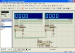 92.3 KB Views: 66
Excellent. Now you need to get the No-Op stuff working.
I'll leave you to do most of the work - just implement the previous C/pseudo code
Hints:
- to write to (just) the first 7219:
- to write to (just) the second 7219:
I'll leave you to do most of the work - just implement the previous C/pseudo code
Hints:
- to write to (just) the first 7219:
Code:
Set CS low
Send No-Op
Send No-Op
Send address
Send data
Set CS high
Code:
Set CS low
Send address
Send data
Send No-Op
Send No-Op
Set CS highUm, I think we're saying the same thing. From the MAX7219 datasheet:(no - the first 16 bits sent end up in the second chip, the last 16 bits end up in the first chip. Imagine the 7219s are in a pipe - you bits you send go through the first chip and into the second.)
Pin 24 -> DOUT -> Serial-Data Output. The data into DIN is valid at DOUT 16.5 clock cycles later. This pin is used to daisy-chain several MAX7219/MAX7221’s and is never high-impedance.
I was off 0.5 clock cycles.
Falcon5252
Member
Why Use Two MAX7219's
Being the MAX7219 Is a eight digit display IC and you want two 4 digit displays, Lets say display two 4 digit ADC values.. Why Not Parallel the segments on two 4 digit displays and multiplex the eight CC digits 0 to 7 the chip is capable of..
Is there any reason the first ADC value could not be displayed on digits 0 to 3 on the first 4 digit display and the second ADC displayed on the second display digits 4 to 7..
I don't understand the constant use of two MAX7219's to run two 4 digit displays.. The only bugs I see is maybe lower display brightness, But the chip has compensation circuitry for brightness, And as far as I can tell multiple decimal points are allowed by setting bit D7 on any or all digits
Anybody see a reason this can't be done with a good outcome...
I can't answer for why DUECINO used the first four digits on each display (post #15) and so had to use 2 MAX's to get 8 digits - maybe there were other things on the second four digits of each display.
Maybe I'm confused - how about a schematic?
I don't see a constant use of two MAX's for thisFalcon5252 said:I don't understand the constant use of two MAX7219's to run two 4 digit displays
I don't really understand the "why not" bit - that would be the completely standard way of using a MAX7219. It doesn't matter if you have 8x1 displays, 2x4 or 6+2 or whatever - all segments are "in parallel" and the common cathodes are connected to the MAX7219 DIGx pins.Falcon5252 said:Why Not Parallel the segments on two 4 digit displays and multiplex the eight CC digits 0 to 7 the chip is capable of..
Maybe I'm confused - how about a schematic?
Falcon5252
Member
You got it right.. I was just making a general statement.. Ive seen the use of multiple MAX7219 when one would suffice, Not just here on the forum, But in commercial devices, Slots machines, Pinball, and other equipment, And it just struck me as strange not to use the chips full capability...
I just wanted to know if I was missing something, And there wasn't some hidden defect in the chip that forced that decision.. Such as excessive flickering, overheating or early failure when driving 8 digits..
I just wanted to know if I was missing something, And there wasn't some hidden defect in the chip that forced that decision.. Such as excessive flickering, overheating or early failure when driving 8 digits..
Two chips for 8 displays is just bad design.
There's no flickering with 8 displays (and the multiplexing is so fast that you can't even see it when shaking the displays in the dark...the standard test for spotting slow multiplexing)...or overheating. I've not had one fail yet.
I've gone off the MAX7219 a bit now (shock! horror!), but only because of the price. I now use the AS1107 (now SOIC only, although I think there's some runout PDIPs available) - pin and software compatible (and actually more functionality if you want it, but I've never used it). Also a bit harder to find....but worth it in a product situation.